MAGAZINE

October
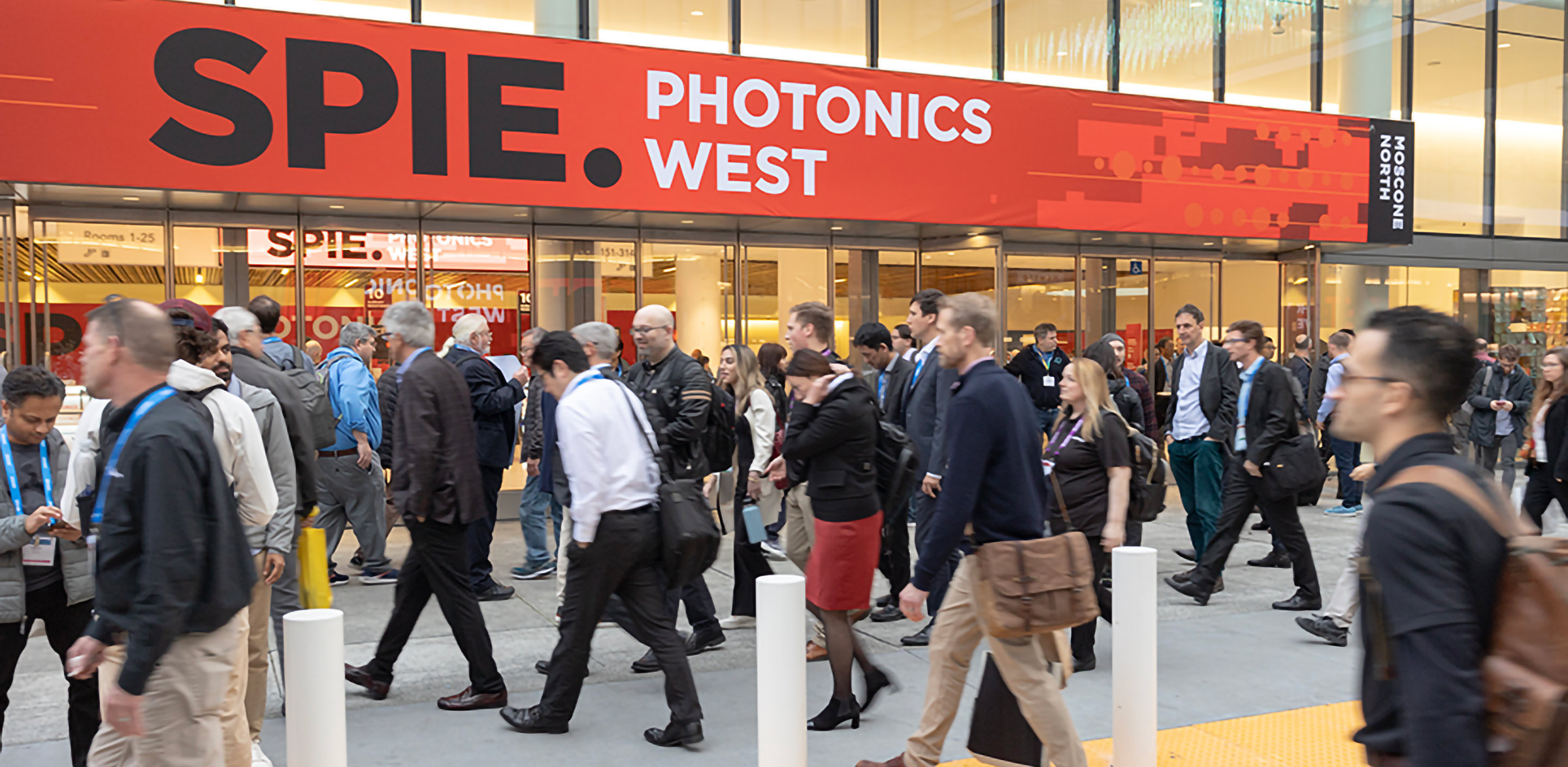

SPIE Photonics West 2025 Now Open for Registration
This year, the week will include 4,500-plus technical presentations across more than 100 technical conferences, as well as hosting over 1,200 companies in four focused exhibitions.
HKU Engineering Team Develops Soft Microelectronics Technologies Enabling Wearable AI for Digital Health
Leveraging rapid technological advances for human health is a global trend, driving the rise of biomedical engineering research. A fast-rising field is wearable biosensors, which have the potential to realise digital healthcare and AI medicine.
SEMICON Japan 2024 to Expand Scope with Spotlight on Advanced Design Innovation
SEMICON Japan 2024, the largest gathering of leaders from the microelectronics manufacturing supply chain in Japan, will assemble more than 1,000 exhibitors showcasing semiconductor solutions for smart technologies from Dec. 11-13 at Tokyo Big Sight.
Infinera’s Planned Expansion Enhances Lehigh Valley’s Legacy of Technological Innovation
Infinera announced it has tentatively agreed to receive up to $93 million in federal funding to expand operations, including in the Lehigh Valley.
Hemlock Semiconductor to Significantly Expand U.S. Production Capacity of Semiconductor-Grade Polysilicon
Today, the Biden-Harris Administration announced that the U.S. Department of Commerce and Hemlock Semiconductor (HSC) have signed a non-binding preliminary memorandum of terms (PMT) to provide up to $325 million in proposed direct funding under the CHIPS and Science Act.
Gartner Identifies the Top 10 Strategic Technology Trends for 2025
Gartner, Inc. today announced its list of 10 top strategic technology trends that organizations need to explore in 2025. Analysts presented their findings during Gartner IT Symposium/Xpo, taking place here through Thursday.
Kioxia to Unveil Emerging Memory Technologies at IEDM 2024
Kioxia Corporation today announced that the company’s research papers have been accepted for presentation at IEEE International Electron Devices Meeting (IEDM) 2024, a prestigious international conference to be held in San Francisco, USA, from December 7th to 11th.
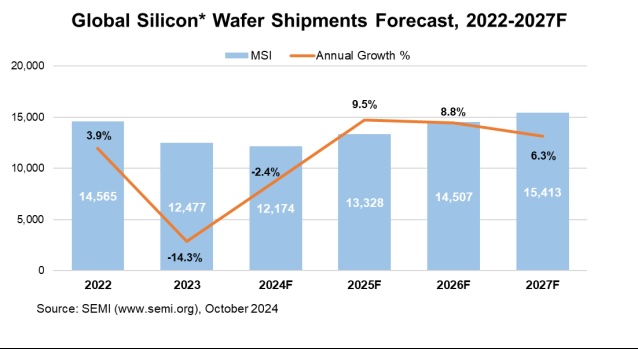
Global Silicon Wafer Shipments to Remain Soft in 2024 Before Strong Expected Rebound in 2025, SEMI Reports
Global shipments of silicon wafers are projected to decline 2% in 2024 to 12,174 million square inches (MSI) with a strong rebound of 10% delyated until 2025 to reach 13,328 MSI as wafer demand continues to recover from the downcycle, SEMI reported today in its annual silicon shipment forecast.
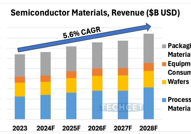
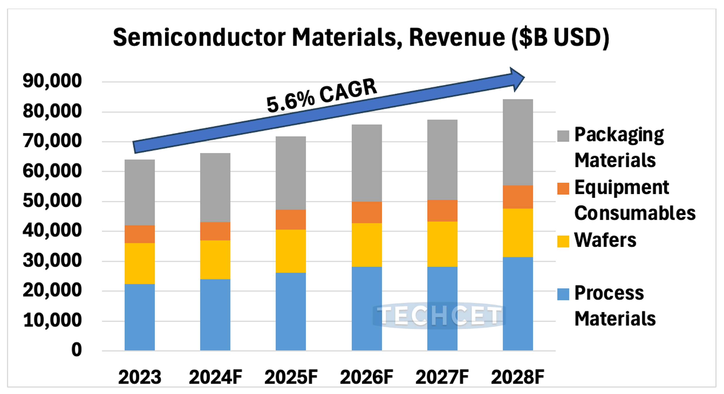
Process Materials Lead the Way in 2024 with 7% CAGR through 2028 Amid Global Challenges
Following a 12% year-over-year decline in 2023 driven by a sluggish industry and inventory correction, revenues for total materials in 2024 is expected to see 3-4% growth as conditions improve.
Arteris Network-on-Chip Tiling Innovation Accelerates Semiconductor Designs for AI Applications
Arteris, Inc. today announced an innovative evolution of its network-on-chip (NoC) IP products with tiling capabilities and extended mesh topology support for faster development of Artificial Intelligence (AI) and Machine Learning (ML) compute in system-on-chip (SoC) designs.
POET Wins “Best in Artificial Intelligence” Honors at 2024 Global Tech Awards
The honor is the third top prize the Company has received in 2024, following recognition by the AI Breakthrough Awards for “Best Optical AI Solution” and the Gold Prize for “AI Innovator of the Year” from the Merit Awards.
SEALSQ and Allion Japan Inc. Partner to Help IoT Device Manufacturers Build Secure, Standard-Compliant Products
The partnership aims to assist IoT device manufacturers in creating secure and standard-compliant products, meeting key protocols such as Matter, and complying with new international IoT security regulations like the EU Cyber Resilience Act (CRA) and the US Cyber Trust Mark.
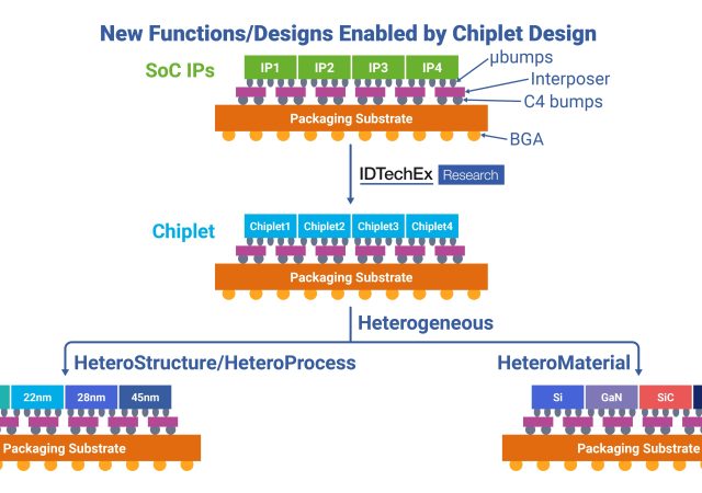
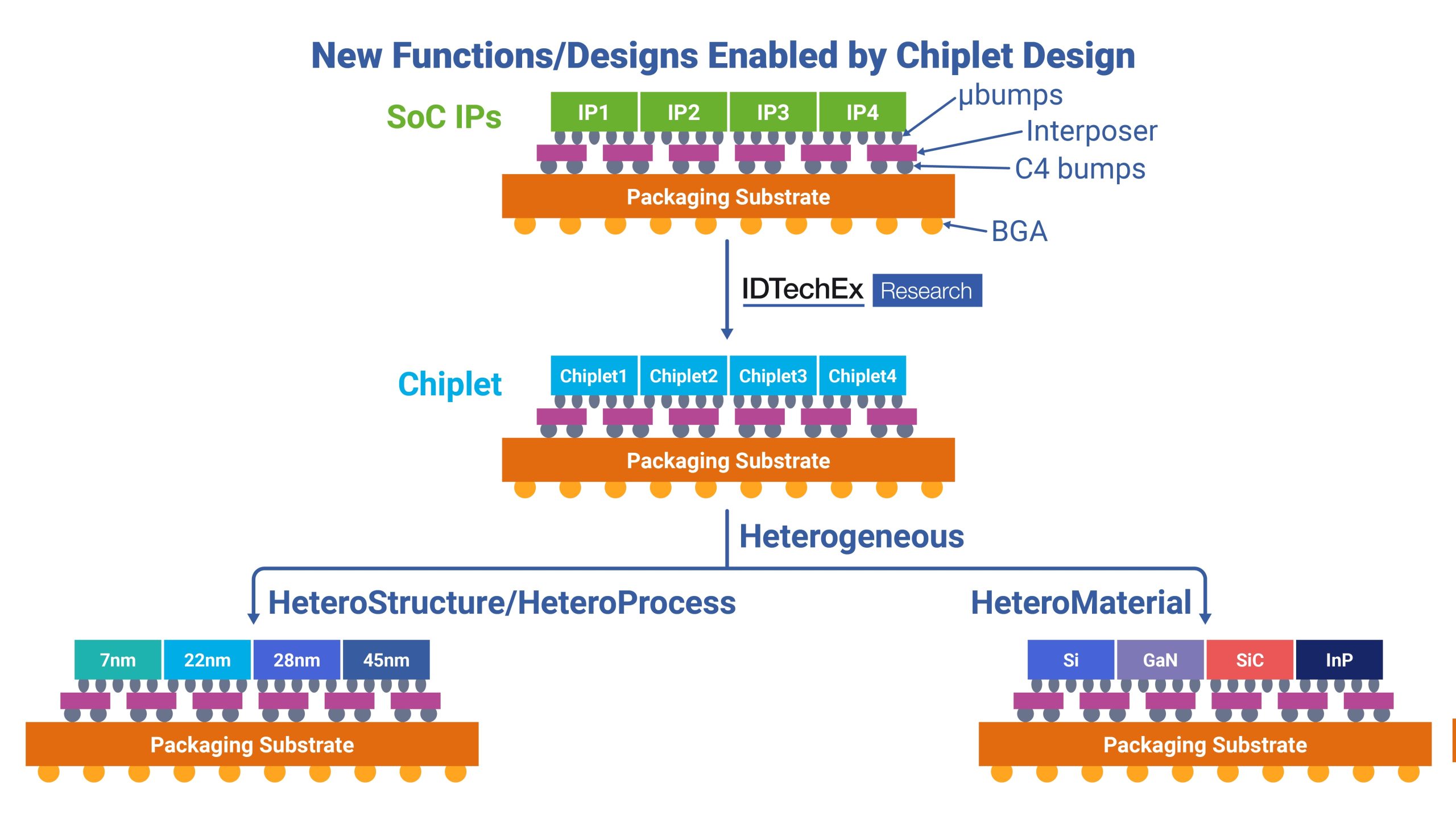
IDTechEx Report Highlights the Rise of Chiplet Technology in Semiconductors
The report highlights how chiplets offer a promising path forward, providing flexibility, modularity, customizability, efficiency, and cost-effectiveness in chip design and manufacturing.
CEA-Leti Launches OpenTRNG
CEA-Leti today announced an open-source project to produce physical True Random Number Generators (TRNG) using ring-oscillator-based architectures.
Samsung Develops Industry’s First 24Gb GDDR7 DRAM for Next-Generation AI Computing
Samsung Electronics Co., Ltd. today announced it has developed the industry’s first 24-gigabit (Gb) GDDR7 DRAM.
Microchip’s RTG4 FPGAs with Lead-Free Flip-Chip Bumps Achieve Highest Space Qualification
QML Class V designation recognizes exceptional reliability and longevity for critical space missions.
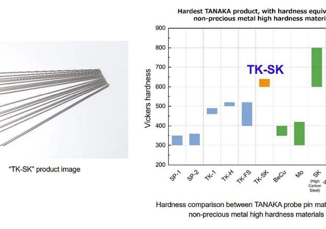
TANAKA Announces “TK-SK” Palladium Alloy for Semiconductor Test Equipment
New palladium alloy with a Vickers hardness of 640HV reduces wear-related deformation of probe pins, contributing to longer service life and lower costs for semiconductor test equipment.
Infinera Receives CHIPS and Science Act Funds to Support Development of Semiconductor Technology Important for Communications and National Security
Today, the Biden-Harris Administration announced that the Department of Commerce and Infinera have signed a non-binding preliminary memorandum of terms (PMT) to provide up to $93 million in proposed direct funding under the CHIPS and Science Act.
Micron Fuels New Wave of AI PCs With Launch of Ultra-Fast Clock Driver DDR5 Memory Portfolio
Micron Technology, Inc., today announced the availability of a brand-new category of clock driver memory with the launch of its Crucial DDR5 clocked unbuffered dual inline memory modules (CUDIMM) and clocked small outline dual memory modules (CSODIMM), which are now shipping in volume.
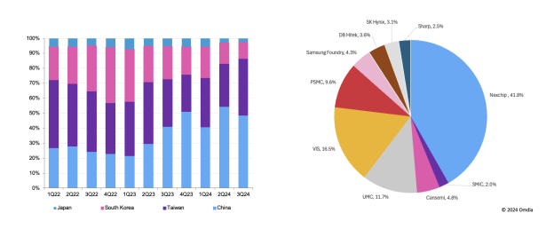
Omdia: NexChip and Samsung Foundry lead LCD and OLED driver IC markets in 3Q24
Latest insights from Omdia’s Display Driver IC Market Tracker indicate that NexChip and Samsung Foundry have emerged as key leaders in the display driver IC (DDIC) market for 3Q24.
SEMI Energy Collaborative Releases Recommendations for Expanding Low Carbon Energy in Taiwan
SEMI, the global industry association representing the semiconductor and electronics design and manufacturing supply chain, today released a report by its Energy Collaborative (EC) with recommendations on expanding low-carbon energy (LCE) availability in Taiwan.
KLA Unveils Comprehensive IC Substrate Portfolio for a New Era of Advanced Semiconductor Packaging
Today KLA Corporation introduced the industry’s widest breadth of process control and process-enabling solutions for IC substrate (ICS) manufacturing.
Forge Nano Receives $10M Investment from GM Ventures
GM plans to utilize Forge Nano’s Atomic Armor surface engineering platform technology to pursue battery cathode material enhancements.
Featured Video
Marposs offers a complete range of non-contact sensors used for thin-film metrology, wafer dimensional characterization, wafer inspection and packaging inspection. The company’s sensors can work inside automatic inspection machines to find defects and dimensional variation. At SEMICON West 2024, Editor-in-Chief Pete Singer talked to Frank Powell, business development manager at MARPOSS about new solutions for the semiconductor industry and the Solarius line of 3D measurement technology, including the new Polaris and Polaris Plus 3D systems.

Semiconductor Daily Digest in your inbox
Featured Products


U.S. Aims for 20% of World’s Leading Edge Semiconductor Production by 2030
Secretary of Commerce Gina Raimondo believes investments in leading-edge logic chips manufacturing will put the U.S. on track to produce roughly 20 percent of the world’s leading-edge logic chips by the end of the decade.


Water Supply Challenges for the Semiconductor Industry
The energy-hungry nature and large carbon footprint of semiconductor manufacturing have received considerable attention in the context of reducing our emissions of planet-warming greenhouse gases. It turns out we are just as thirsty as we are hungry.


")

Professors from MIT, UCLA to be Honored for Excellence in Semiconductor Research
The Semiconductor Industry Association (SIA), in collaboration with the Semiconductor Research Corporation (SRC), today announced the winners of its 2019 University Research Awards.

What Do Small Companies Need to Know about the CHIPS Act?
IBM’s Poughkeepsie, N.Y. site was the backdrop for one of President Biden’s speeches promoting the passage of the $52B CHIPS (Creating Helpful Incentives to Produce Semiconductors) and Science Act, a rare piece of legislation for which the president won bipartisan support.


Intel 4 Process Drops Cobalt Interconnect, Goes with Tried and Tested Copper with Cobalt Liner/Cap
At the VLSI Symposia in June, Intel presented a paper “Intel 4 CMOS Technology Featuring Advanced FinFET Transistors Optimized for High Density and High-Performance Computing.” Blogger Dick James reports on details of the interconnect strategy.


EVENTS
October
November
December