By David Fried
Semiconductor process development is no easy task, with each generation of devices more difficult and expensive to create. Traditional cycles of build-and-test development are becoming obsolete, since they are too expensive and time-consuming for the most advanced processes.
The High Cost of Process Development
Most chip designers developing new products rely on existing manufacturing processes, but someone had to create those processes to make the designs possible. The goal of process development is to create new semiconductor manufacturing processes that provide high yield while achieving the required device performance. In contrast to new chip design, however, it requires an entirely different set of engineers and skills.
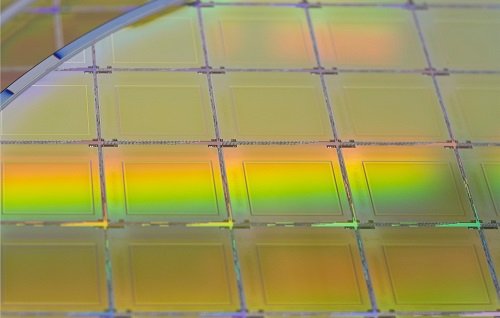
The traditional approach to process development involves building multiple test wafers to determine the ideal process for a given device. After one set of wafers is fabricated and analyzed, insights from the previous round help to refine process steps for another round of fabrication. Due to smaller feature sizes, each new process generation is more sensitive to variation. This adds even more complexity because smaller feature sizes and parasitic effects require more measurements and testing as well as additional fabrication. The cycle is repeated many times before the entire process flow can be finalized, making it time- and cost-intensive, especially for the most advanced technology nodes.
Testing Virtual Wafers Instead of Real Wafers
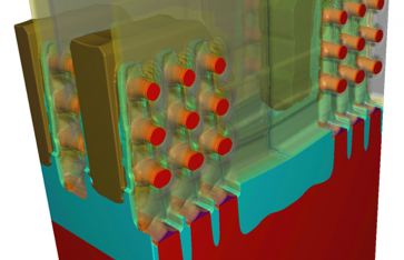
Today, there is an alternative to this slow, expensive way of doing things. Virtual fabrication lets computers simulate all of the processing that occurs when real wafers are built. These virtual models allow semiconductor process engineers to test manufacturing equipment settings with far greater variation than is possible in a physical fab. Designers can simulate the entire process flow, running the equivalent of thousands of wafers in days instead of months. Designers can quickly see graphical animations to visualize process steps, modify process recipes and device geometries, and measure how these changes affect electrical behavior.
Improving Yield Using Statistics in Virtual Wafer Fabrication
Because of the high volume of data generated, designers are turning to statistical analysis to provide greater confidence in their choice of process settings. Defects and random variations can be modeled in a virtual fab in a way that’s not possible in a real fab, letting developers test the sensitivity of the device structures against the unpredictable aspects of processing.
There’s more than one approach to optimizing the process settings used in a new memory or logic fabrication sequence. The simplest one involves taking a single variable and exploring its effects. Critical dimensions (CDs), for example, establish those feature sizes of a device that ensure desired electrical performance. A particular dimension can be swept from low to high values – developers can then measure the effects of that range on device behaviors such as threshold voltage. This allows developers to ensure that the electrical behavior of their device design addresses the range of expected feature sizes and variability. The interactions with intersecting process steps can also be tested for further validation, since these interactions can lead to unanticipated device performance.
But, in reality, this approach isn’t sufficient for studying the complex web of interactions between process steps and the resulting structures.
A second approach leverages Monte Carlo analysis, randomly varying a wide range of process and device parameters and calculating the resulting device geometry and performance. This data can be used to automatically identify the process and design settings needed to achieve yield and performance goals. It’s an area where simulation shines, providing a useful way to test the interactions between many different processes.

Virtual Fabrication Platform
SEMulator3D is a virtual fabrication platform created by Coventor, a Lam Research company. It allows the definition of all process steps, the modeling of devices, the collection of metrics, electrical and device analysis, the statistical analysis of results, and the visualization of process steps through graphical animation. Today, semiconductor companies use it for both optimizing and scaling leading process nodes and for developing advanced new technologies like GAA (Gate-All-Around) transistors.
The ability to do this work virtually is the future of semiconductor process development. Virtual fabrication accelerates new process time-to-market by months, opening up market opportunities worth hundreds of millions of dollars for semiconductor companies.

To learn more about virtual fabrication and how it’s changing the future of semiconductor technology development, download our whitepaper Speeding Up Process Optimization with Virtual Fabrication.
Lam Research is a longtime member of MEMS & Sensors Industry Group®, (MSIG), a SEMI technology community that connects the MEMS and sensors supply network in established and emerging markets, enabling members to grow and prosper. Visit us today.
David M. Fried, Ph.D., is vice president of Computational Products at Lam Research, where he is responsible for the company’s strategic direction and implementation of virtual process solutions, including the Coventor SEMulator3D virtual fabrication 3D process modeling solution. Fried leads the execution of technology strategy for technology platforms, partnerships, and external relationships. His expertise touches upon such areas as Silicon-on-Insulator (SOI), FinFETs, memory scaling, strained silicon, and process variability.
Fried is a well-respected technologist in the semiconductor industry, with 60 patents to his credit and a notable 14-year career with IBM, where he was involved in successive process generations from 65-nanometer and lower. His most recent position was 22nm chief technologist for IBM’s Systems and Technology Group. He holds bachelor’s, master’s and doctoral degrees in Electrical Engineering from Cornell University.
