By JEONGDONG CHOE, Senior Technical Fellow, TechInsights, Ottawa, Canada
A new 3D QLC NAND product has just arrived. TechInsights has quickly reviewed the Intel 1Tb QLC die removed from SSD 670p series which use 144L 3D NAND devices. The SSD 670p (Model: SSDPEKNU020TZ 2.0TB, 144L QLC, SM2265G controller) is Intel’s third generation of consumer NVMe SSD to use QLC (Quad Level Cell) NAND, following the SSD 660p (64L QLC, SM2263 controller) and SSD 665p (96L QLC, SM2263 controller). It’s a single-sided M.2-2280 PCIe 3.0 x4, NVMe 1.4 with Nanya NT5CC128M16JR-EK 256MB DDR3L-1866 DRAM cache to improve read and write latency, and throughput as well. Intel announced 670p’s write endurance is 23% higher than the 665p SSD and 85% higher than the 660p SSD. The new 144L QLC die is still manufactured with the same 1Tb capacity per die as the 64L QLC and 96L QLC.
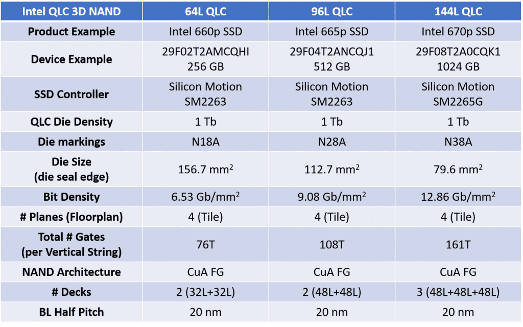
Two 29F08T2A0CQK1 devices are packed on SSDPEKNU020TZ together, and eight 144L QLC dies are stacked in each device with N38A die markings. Die size decreased to 79.6 mm2 which is 50% of 1Tb 64L QLC N18A die and 70% of 1Tb 96L QLC N28A die. Intel designed it with 144L (144L-tier), floating gate (FG) storage node, 4-plane architecture with CMOS under Array (CuA) to increase sequential read and program parallelism without area penalty. Bit density also increased to 12.86 Gb/mm2, which is around 2x higher than the N18A die and 1.4x higher than N28A die. Table 1 shows a comparison of Intel 3D NAND QLC FG products; 64L, 96L and 144L.

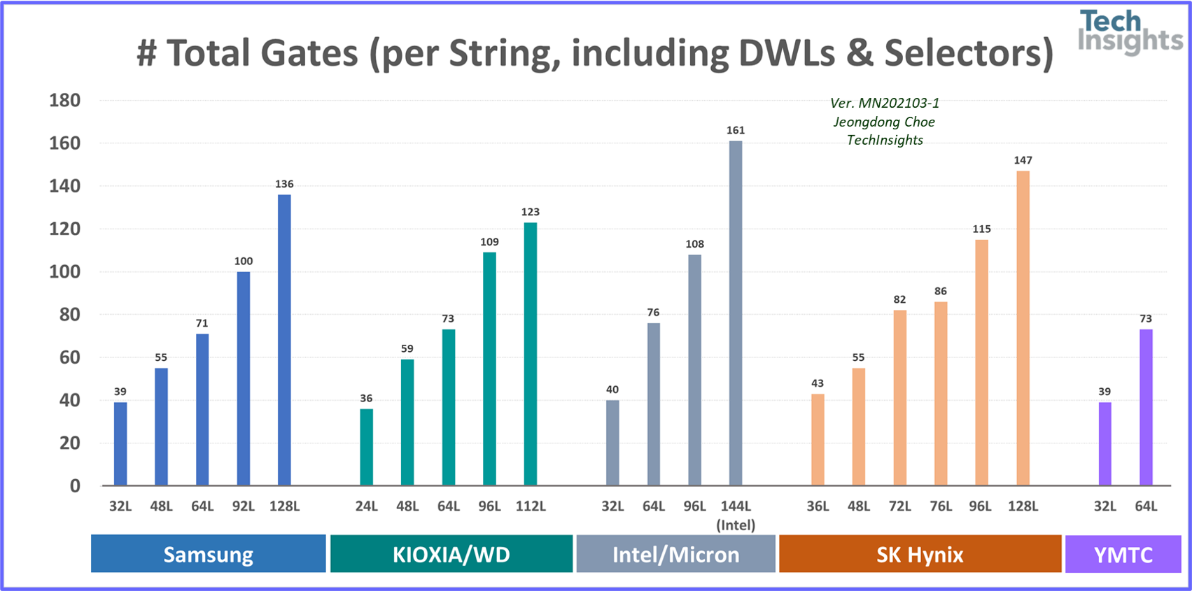
Intel (PF2KX038TZO 3.84 TB) TLC SSD products also use the same N38A die with SSD 670p QLC chips. Intel embedded EAX33339 controller for D7-P5510 TLC SSD, while we found SM2265G controller from 670p QLC SSD. The die might be designed to be operated with either TLC (virtually 768Gb) or QLC (1Tb). Intel 144-tier NAND string consists of three decks (upper deck, middle deck, lower deck) between source and bitline, which is different from their previous 64L (2-deck) and 96L (2-deck) structures. By dividing the 144 tiers into 3 decks, with 48 WLs in each deck, the block size is reduced to 48MB. Decks can be assigned to any combination of QLC or SLC blocks to fully benefit from Intel’s new block-by-deck concept in the storage system.
The full article appears in the April/May issue of Semiconductor.
