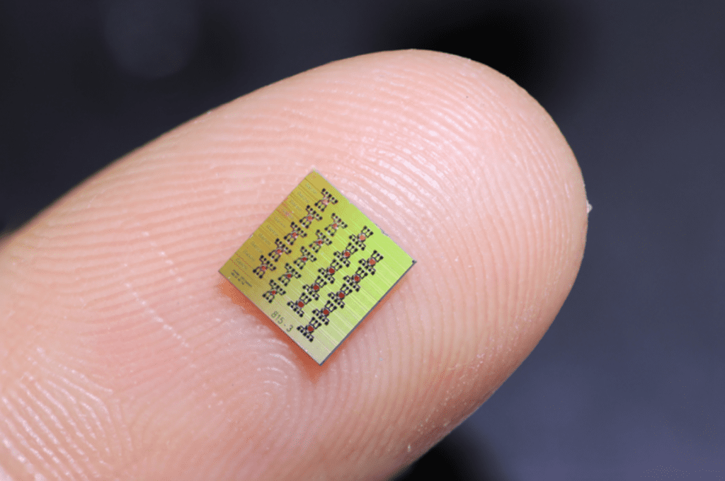
Integrated photonics allow us to build compact, portable, low-power chip-scale optical systems used in commercial products, revolutionizing today’s optical datacenters and communications. But integrating on-chip optical gain elements to build lasers or to amplify optical power runs the risk of reflected light from other components compromising or interfering with the laser’s performance.

The solution is to increase on-chip optical isolation. Typically, optical isolation is achieved with magnetic materials and magnetic fields, but these are not compatible with current semiconductor foundry processes; meanwhile, creating strong external magnetic fields on the chip’s micrometer scale is challenging in itself. Consequently, electrically driven, magnet-free optical isolators are highly desired in the field.
In an article published in Nature Photonics, a collaboration between the labs of Professor Tobias J. Kippenberg at EPFL and Professor Sunil A. Bhave at Purdue University showcases such a magnetic-free, electrically driven optical isolator that enables light routing on a chip.
Combining integrated photonics and micro-electromechanical systems (MEMS) technology, the device is made using piezoelectric aluminium nitride (AlN) monolithically integrated on ultralow-loss silicon nitride (Si3N4) photonic integrated circuits.
By synchronously driving multiple piezoelectric MEMS actuators, bulk acoustic waves are generated electromechanically, which can couple to and deflect light propagating in the Si3N4waveguide beneath them. This acousto-optic modulation, known as “spatio-temporal modulation”, mimics the effects of magnet-driven isolators. By replacing magnetic materials with piezoelectric thin-film transducers, the requirement of magnetic field is entirely avoided.
While magnetic-free optical isolators have been shown before, this is the first one that is driven electrically and operated in the linear optical regime. The study reports linear optical isolation of 10 dB, and experimental measurement of one-way, no-loss digital data transmission on an optical signal carrier.
“Combining integrated photonics and MEMS engineering, we show a hybrid semiconductor fabrication technology that is fully CMOS-compatible and accessible via large-volume foundry processes,” says Dr Junqiu Liu who leads the fabrication of Si3N4 chips at EPFL’s Center of MicroNanoTechnology (CMi).
The new optical isolators can seed new applications including chip-scale atomic clocks, light detection and ranging (LiDAR), photonic quantum computing, and on-chip spectroscopy, among others. One particular application that the two teams are working on is building quantum coherent microwave-to-optic converters that could conquer efforts in quantum interconnects between distant superconducting qubits, which require conversion of single quanta of the microwave field to the optical domain and vice versa.