Paul Farrar, general manager of the G450C consortium, said early work has demonstrated good results and that he sees no real barriers to implementing 450mm wafers from a technical standpoint. Speaking at the SEMI ISS meeting in January, Farrar showed impressive results from, etch, CVD, PVD, CMP, furnaces, electroplating, wet cleans and lithography processes and said the inspection/metrology tools were in place to measure results. “I don’t believe we will find fundamental technology limiters,” he said. “But we will have to keep working to find ways to maximize the efficiency.” Gaining such efficiencies are critical in order to meet the cost-saving goals of the program. “In the end, if this isn’t cheaper, no one is going to do it,” he said.
G450C is a consortium based at the CNSE campus in Albany, NY. It is financed by Intel, TSMC, Samsung, IBM, GLOBALFOUNDRIES, and New York State (CNSE). “Our job is to make it as easy as possible to innovation and be collaborative between the semiconductor makers and our key friends in the industry who enable the 450 work to be done in an economic way,” Farrar said.
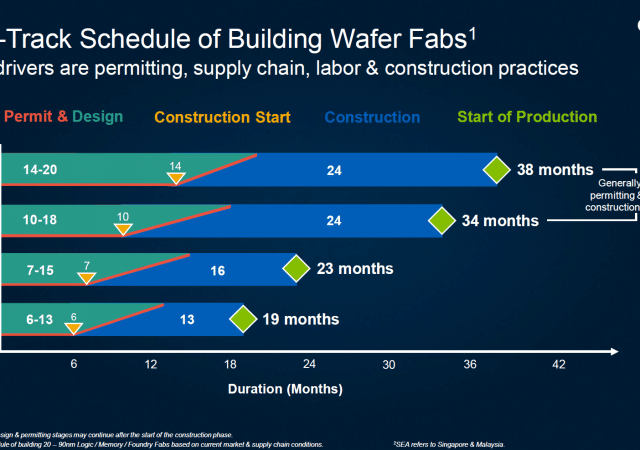
At the end of 2013, G450C at 34 tools delivered to its 50,000ft2 fab in Albany, with another 7 tools in place at partner’s facilities. “The FOUPS are going, the overhead transport is well underway and some of the cleanroom is actually starting to look like a cleanroom,” Farrar said.
Farrar started with etch results, saying they were “starting to see some pretty good data – 3 sigma at about 2%. Yes, there’s still some work to get to the very edge of the wafer but relatively good progress and good jobs on gas delivery, etc.
He showed good results with both oxide and silicon nitride CVD, with close to 1.5mm edge exclusion. “It’s very representation data from early in the program,” Farrar said, noting that they were starting to pattern some of the more complex oxides.
He said the goal for PVD was to demonstrate better than 5% uniformity. “We know we have step coverage challenges for both the 10 and 7nm nodes. There’s tremendous work going on in the injection rings for gases, high density plasmas from multiple RF sources, but again some progress to me made but pretty good data for right out of the chute,” he said.
CMP results demonstrated repeatability less than 4%. “Very good job done by our suppliers,” Farrar said.
Farrar described data from furnaces as reasonably good. “We still need to do more characterization at what I call the micro level,” he said. “We see some hot spots on the edge, but we’re starting to work on those.”
Also “pretty good data” from electrochemical plating (ECP) of copper. “Well done here,” Farrar said. “The challenge is thermal and pattern loading effects, and gap fill.”
More of the same with wet cleans. “We’re starting to see some pretty good particle data. We’re cleaning wafers relatively well. We are seeing a few things like what I would call micro-metallic contamination that can grow some things so we’re still working on that. But from a particle removal standpoint, pretty good unit process work,” Farrar said.
Farrar acknowledged that lithography remained as one of the biggest challenges in the 450mm transition, but showed good results from directed self assembly across a 450mm wafer, and said the consortium had a very strong partnership with Nikon. “We’re working with them and we’ve seen some tremendous progress at their factory,” he said. “I’m fully confident that we’ll have capability by July to run patterned wafers. Immersion is going to be the workhorse. I think that’s a key enabler to get to 450mm.” He said the industry would have to see how the economics of EUV played out later in time. “I don’t think it’s going to be early in time,” he said.
Farrar seemed to draw hope from the earlier transition from 200mm to 300mm wafers, which started around 1998. “By 2008, we were getting more than 2X the number of wafers per tool out compared to what was going in 2003. There was about a 70% improvement over 5 years,” he said.


