To make computer chips — and the devices they power — even smaller and more efficient, engineers need new materials.
Three University of Texas at Dallas faculty members and collaborators from other universities and two industry partners have teamed up to design and test indium-based materials to enable the manufacture of the next generation of computer chips.
The researchers have received a $1.9 million, three-year grant to support their work through the National Science Foundation Future of Semiconductors (FuSe2) program.
The UTD funding is part of $42.4 million in FuSe2 grants announced in September to support the goals of the federal CHIPS (Creating Helpful Incentives to Produce Semiconductors) and Science Act of 2022 to make microchips more energy efficient and to facilitate the domestic production of integrated circuits.
By introducing indium-based materials, the researchers aim to facilitate patterning in the extreme ultraviolet (EUV) range. Patterning, or lithography, is a key step in the semiconductor fabrication process in which patterns are created on the surface of a wafer to serve as pathways for transistors and other components. Moving from deep UV to EUV range makes it possible to produce smaller, more precise features on chips for better performance and energy efficiency.
During the traditional patterning process in semiconductor manufacturing, silicon wafers are coated with a removable layer of material called a photoresist before being exposed to UV photons. The next generation of lithography uses very high-energy photons — 92 electronvolts — in the EUV region. Due to the high energy of these photons, conventional photoresist materials will not work.
The researchers’ new materials also could enable the production of 3D circuits, which are designed by stacking layers of chips like high-rises in a crowded city. New materials are needed to build added layers on a 3D chip without disturbing the existing circuits.
“If you are making a layer of devices on top of another layer of devices, you cannot heat it to a high temperature. Otherwise, you will destroy the existing layers,” said Dr. Julia Hsu, professor of materials science and engineering, the Texas Instruments Distinguished Chair in Nanoelectronics in the Erik Jonsson School of Engineering and Computer Science, and principal investigator of the project.
Hsu said using indium-containing materials for the EUV photoresist and the transistors should lead to more efficiency by eliminating a step in integrated circuit manufacturing that involves solvents. Hsu is testing a technique called photonic curing to convert EUV patterned structures to nanoscale devices. Photonic curing uses pulses of light at high intensity but low energy to complete the chemical reactions that allow the indium oxide to achieve better semiconducting properties without overheating the underlying devices.
Hsu’s preliminary work on indium-containing materials as an EUV photoresist has been supported by a Semiconductor Research Corporation (SRC) grant to investigate new semiconductor materials. She also plans to incorporate machine learning — a method she learned with support from a 2023 Simons Foundation Pivot Fellowship — into the project’s design and testing methodologies.
“The FuSe2 project will enable us to take our preliminary results from the SRC project to a much higher level and bigger impact,” Hsu said. “We will bring computation and synthetic chemistry to expand beyond currently commercially available materials.”
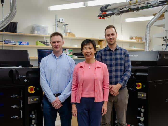
Hsu’s co-principal investigators include Dr. Cormac Toher, assistant professor of materials science and engineering and a computational materials scientist, and Dr. Kevin Brenner, assistant professor of materials science and engineering. Toher will design the indium-containing molecules, and Brenner will fabricate and test the devices.
The UTD researchers are working with co-principal investigators Dr. Howard Katz, professor of materials science and engineering at Johns Hopkins University, who will synthesize new molecules designed by Toher; and Dr. Chih-Hao Chang, associate professor of mechanical engineering at UT Austin, who will perform EUV testing on new photoresist materials; and collaborators at Tokyo Electron, Coppin State University and Northrop Grumman.
The project also includes semiconductor industry workforce training for community college students through UTD’s North Texas Semiconductor Institute and a class that Hsu will teach as an immersive experience in the semiconductor industry.
