NELSON FAN and GREG CLEMONS, ASMPT
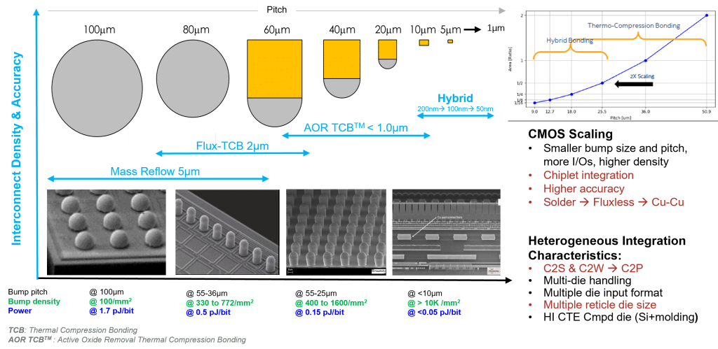
The scaling of complementary metal-oxide-semiconductor (CMOS), under the driving forces of high-performance computing (HPC) and artificial intelligence (AI) applications, has successfully showcased the possibilities of “more than Moore” via the heterogeneous integration (HI) of chiplets in various advanced package architectures, in tandem with advanced first-level interconnect (FLI) technologies (FIGURE 1).

These advanced package architectures consistently deliver comparable or improved device performance relative to system-on-chip (SoC) formats, while achieving the accelerated time-to-market and the best cost of production. The fluxless thermal compression interconnect process with active oxide removal (AOR) by plasma continues to facilitate high yield pitch scaling by eliminating flux, flux residue, and costly cleaning solutions that inflate total cost of ownership (TCO). AOR technology empowers chiplet integration and high bandwidth memory (HBM) devices with fine bump pitch roadmaps and new package architectures, while also being backward compatible with large-size-and-pitch packages typically susceptible to warpage.
Chiplets and HBM stacks with higher density and I/O counts at a finer pitch (down to sub-micron pitch levels) drive the advanced packaging process development around AOR technology. The deployment of the AOR approach aims to improve package interconnect yield at both finer pitch levels and overall larger package sizes. To achieve the required device performance, a very high degree of chiplet placement accuracy in a HI device is being scaled up, and more advanced FLI processes developed. Transitioning from traditional mass reflow flip-chip (MR-FC) and thermal compression bonding (TCB) with placement accuracy of 5µm and 2µm respectively, the technology is now evolving towards AOR TCBTM (active oxide removal thermal compression bonding) with bond accuracy of less than 1µm to address very high bump densities, with pitches targeting at less than 10µm. Moreover, hybrid bonding technology that targets devices with higher densities and better yields at an affordable cost of ownership for high-volume manufacturing (HVM) will soon also be able to leverage AOR technology. AOR processing is thus set to further enable solder FLI pitch scaling, transitioning into an in-situ cleaning solution for hybrid bonding applications.
AOR Applications
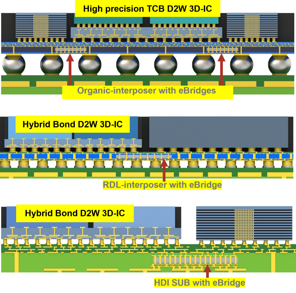
Over the last decade, various HI package architectures have been developed by technology frontrunners, including wafer foundries, integrated device manufacturers (IDMs), outsourced semiconductor assembly and test suppliers (OSATs), and advanced substrate houses (Figure 2). These HI package architectures can be classified into three major, basic categories: 1) through-silicon via (TSV) interposer; 2) redistribution layer (RDL) interposer; and 3) single and/or multiple embedded silicon bridges (e-bridge) inside the high-density build-up interconnect (HDI) substrate. Each of these has its unique requirements for developing integrated AOR solutions.

