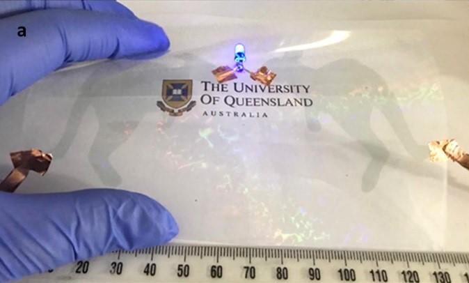
Australian researchers have demonstrated the strong potential for a new type of flexible, recyclable electrodes to be used in creating cheaper solar cells, touchscreens, wearable ‘e-skins’ and next-generation responsive windows.

These materials, made using a simple, cost-effective fabrication processes, could replace traditional transparent conductive oxides such as indium tin oxide (ITO), which is a necessary component of almost all thin-film solar cells, laptop screens and smartphone displays, but which is steadily rising in price due its scarcity, and is inherently limited by its brittle nature.
In addition to cheaper, high-efficiency photovoltaic solar cells, computer displays and smartphone touch screens, household energy bills could be slashed in the long-term, with the electrodes potentially able to be used in manufacturing smart windows, which can electrically shift colour and become opaque or transparent.
Contributing author Dr Eser Akinoglu of the ARC Centre of Excellence in Exciton Science said: “The performance of the material is excellent, the transmission of above 90% and high electrical conductivity rivals the ITO benchmark.”
Looking ahead to the potential commercial application of the research, he added: “In principle, you should be able to integrate this technology into industrial roll-to-roll printing.”
Achieved using a technique called nanosphere lithography, a deposition method which involves evaporating the desired combination of materials into a nanoscale pattern, researchers from The University of Queensland and the ARC Centre of Excellence in Exciton Science have published their findings in the journal Advanced Functional Materials.
The dielectric/metal/dielectric (D/M/D) nanomesh electrodes produced through this approach boasted precisely controlled perforation size, wire width and uniform hole distribution, yielding high transmittance, low sheet resistance (which minimises loss of voltage) and outstanding flexural endurance.
Lead author Dr. Tengfei Qiu of the University of Queensland said: “We offered a strategy to make the shadow area of the metallic nanomesh highly transparent, by integrating D/M/D structures to the nanomesh system. The nanomesh transparent films with D/M/D layered structure have not been studied before. The simple and cost-effective nanosphere lithography technique can be applied to fabricate diverse layered nanomesh materials.”
And, in the case of certain flexible electrochromic applications, the electrodes even demonstrated the capacity to be recycled, enhancing the mechanism’s credentials as a possible sustainable alternative to more established manufacturing materials and processes.
Dr Akinoglu said of this recyclable characteristic: “It means that if you make a device like an electrochromic window, which may deteriorate in functionality after its life-span, you can take it apart, flush rinse the electrodes, and reuse them for another device.”
One of the next steps for researchers is to explore the potential shown in this study to create similar results at a larger scale, with a long-term view to achieving similar outcomes in a commercially viable capacity.
“You want to get the transparency higher, you want to get sheet resistance lower and you want to get the endurance for mechanical stress and flexibility higher,” Dr Akinoglu said.
“And you want to be able to fabricate it on a large-scale area, at a low cost.”
Senior author Prof. Lianzhou Wang added: “This work will inspire the design of transparent conductive films with novel functions such as flexibility and recyclability, providing an excellent platform for next generation eco-friendly optoelectronics.”