Keynote speaker at SEMI Pac NW event discussed specific AI use case examples in manufacturing before finishing with TAP and a Cambrian explosion.
By John Blyler, Senior Contributing Editor, Semiconductor Digest
Chip makers are beginning to realize the value generative AI (Gen AI) technology can bring to the manufacture of semiconductor devices. Gen AI is significantly improving the categorization of defects, predicting needed equipment maintenance before breakdowns, and helping workers make real-time adjustments. This can reduce downtime and production costs while leading to greater manufacturing precision.

At a recent SEMI Pacific NW event, Daniel Burlingame, General Manager, and Managing Director at Analog Devices, Inc. (ADI), Beaverton Wafer Fab, discussed the importance of Gen AI in wafer fabrication by first examining the evolution of industrial innovation.
His thought-provoking keynote highlighted AI trends in the fabrication of chips, with theories on the adjacent possible and a comparison to the modern industrial revolution’s Cambrian-like Explosion.
The latest cycle (fifth) of the Industrial Revolution unofficially started ten years ago in 2014. It emphasizes the collaboration of humans and advanced technologies to create a more sustainable and human-centric approach to industrialization. It builds on the digital advancements of the 4th Industrial Revolution with transformations of the industrial structure through the utilization of AI, IoT, big data, etc.,
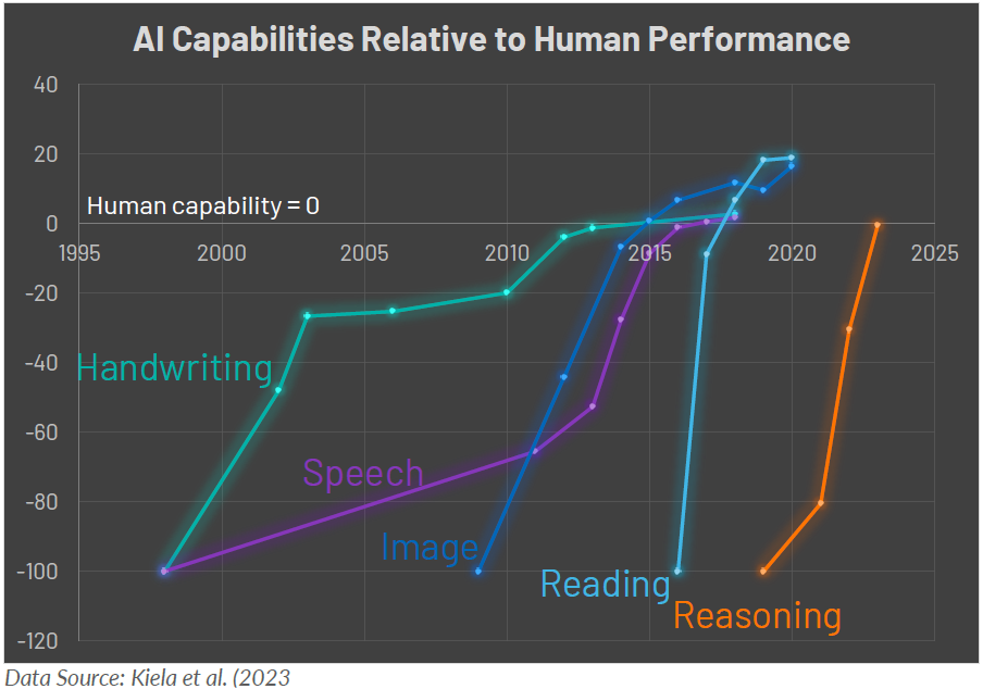
Most early industrial revolutions were marked by abrupt improvements in a country’s GDP following long periods of flat or little growth. Burlingame believes this is happening now as many AI capabilities are finally exceeding those of humans in terms of writing, image recognition, reading, and even basic reasoning (see Figure 1).

Ways AI Helps Semi Fabs
Burlingame cited many ways that AI is helping semiconductor fabrications, starting with defect detection. Gen AI has found defects and associated classification categories more readily than most humans. These classification areas include defects caused by scratches, particles, flakes, fibers, oxide bumps, and non-visual and etch blocks. He presented a slide that plotted a significant improvement in the number of wafers classified weekly by Gen AI vs human defect classification.
“While we solved this without AI, it would have gone a lot faster with it.”
Daniel Burlingame, General Manager, ADI Beaverton Fab
Gen AI significantly increased the number of classifications, which provided the fabs managers and engineers with accurate data upon which to act, e.g., shutting down specific machines and fixing them. In this way, manufacturing professionals can work alongside AI in the factory to improve quality, shorten time, and reduce costs.
Another way AI is helping semiconductor fabs is by reducing equipment downtime. Burlingame indicated that large language Models (LLM) were implemented to classify errors at the ADI fab automatically. Large language models (LLMs) are a type of artificial intelligence (AI) program that can perform natural language processing (NLP) tasks using large amounts of data. Many industries benefit from using LLMs to offer more accurate predictive maintenance capabilities, reducing equipment downtime and maintenance costs.
In practice, the LLMs provide auto-generated error Pareto charts that allow the equipment team to focus on fixing the root causes of down equipment. This idea is to let the LLM go loose on one’s equipment logs to create a praetor for tools going down from numerous defects, e.g., an RF fault. AI can be used to remove the time-consuming, human administrative work of manually going through the logs and classifying all of the errors. This way, the equipment workers can focus mainly on fixing the problem.
The third type of use case for AI in wafer fabs was for process improvements. AI can leverage large datasets for multivariate or high-order correlations. Such correlations extend the concept of pairwise correlations to relationships among three or more variables. When appropriately used, multivariate correlation problem-solving can drop the time for improved results in quarters or years to days. Burlingame provided an insightful example.
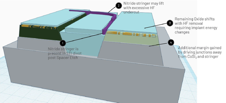
“This problem was difficult to solve,” noted Burlingame. “We experienced diode leakage turn on during parametric test or acceptance test. The diode leakage was correlated to the amount of remaining oxide after the space etch.”
“But that wasn’t the whole story. We realized it was a multivariate problem. This same diode defect would turn on or off with different implant conditions. It wasn’t until we got to model-based problem solving that we could create an image that revealed that a spacer nitrite stringer is present when not fully etched. When your HF undercut and subsequent clean aren’t high enough, the spacer stringer can lift, and implant conditions can get you into or out of that failure regime. In this case, nitride is not fully insulating, so it would bridge between a neighboring P+ region and n well, causing this leakage current. While we solved this without AI, it would have gone a lot faster with it.”

The final area where AI would input wafer fab in yield improvement. If the wafer lot yields below that limit, e.g., three sigma, resulting in a 30% yield loss, then someone must investigate the problem. But what about all the other lots in between, the other perturbations from the baseline?
AI can use multivariant regression to examine production runs using different combinations of manufacturing equipment and processing chambers. With AI, the 30% yield loss from one lot now improves to a recovery of 5% on every lot that runs in the factory.
Adjacent Possible
Digitization, the IoT, and handling large data sets are the essential elements of the fifth industrial revolution. When the manufacturing environment is fully connected to the Internet and uses AI, the operation can be tailored to run in various configurations. For example, the operation could be tuned to maximum efficiency at the expense of power, the lowest electricity usage, or balancing manufacturing efficiency. Almost any factory can now be turned to sustainability goals.
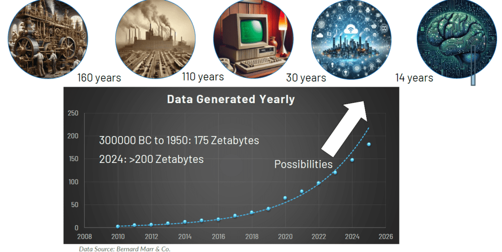
At this point, Burlingame introduced the theory of adjacent possible (TAP), first introduced by Stuart Kaufmann from the University of Pennsylvania. Originally associated with biological systems, the theory predicts a long period of almost no change followed by a hockey stick explosion of growth and connections in a finite amount of time.
He used carbon as an example to help visualize this abstract idea. Carbon, the most abundant element in the human body, formed the basis of the human body about 300,000 years ago. Carbon interacted with other constituents of the body to create humans during what is known as the Cambrian explosion, an event in which a wide variety of animals burst onto the evolutionary scene. But how does that relate to the Industrial Revolution?
Burlingame overlapped the theory of adjacent possible with the Industrial Revolution (IR), noting that it took 300,000 years to reach the first IR, 160 years to reach the second, 110 years to achieve the third, 30 years for the fourth, and 14 years to get the fifth.
This means we live in a Cambrian explosion of technology and an unimaginable amount of data. All the data will require AI to process and handle it, enabling a future we never thought possible and can not fully imagine. But what we do know is that the future is going to make for some very rapid change.