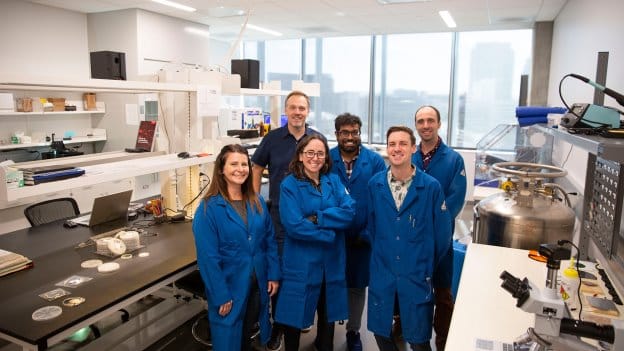
Crystal Sonic, an Arizona State University startup, won first place and $25,000 during the 2024 Natcast Startup Pitch Competition at the National Semiconductor Technology Center, or NSTC, Symposium and Microelectronics Commons Annual Meeting in Washington, D.C. The Shark Tank-style event enabled startups to reach a panel of investors, entrepreneurs and leaders from the semiconductor industry.
Co-founded by Mariana Bertoni, a professor of electrical engineering at Arizona State University, and led by CEO and co-founder Arno Merkle, Crystal Sonic is advancing unique methods to revamp silicon wafer production and improve semiconductor manufacturing.
Crystal Sonic’s successful pitch showcased its innovative acoustic technology to reduce material waste by enabling thin device lift-off and substrate reuse during the semiconductor manufacturing process.
“Winning the pitch competition at the NSTC Symposium is an incredible honor for Crystal Sonic,” Merkle says. “The positive recognition unquestionably validates the critical need in the industry to lower cost and reduce waste for next-generation semiconductors toward sustainable manufacturing.”
Established by the CHIPS and Science Act of 2022, Natcast is a non-profit entity created by the U.S. Department of Commerce to operate the NSTC consortium, which conducts advanced research and development on semiconductors. The CHIPS Act directs an investment of $52.7 billion by the U.S. government into the semiconductor industry aimed at revitalizing U.S. manufacturing.
This marks the second significant competition won by Crystal Sonic this year, as the startup secured a $250,000 investment at the 2024 Lam Capital Venture Competition, an international event inviting participants to solve industry challenges with emerging semiconductor and manufacturing technologies.
“It was amazing to get recognition from the venture capital and semiconductor industries, especially as a small startup,” Bertoni says. “It has resulted in a lot of visibility, and Lam Capital has given us exposure and connected us with other venture capital firms that were part of the judging for the competition.”
Sound alternative to unwanted waste
One of Crystal Sonic’s primary goals is to reduce waste and lower costs in the production of next-generation semiconductor devices. Existing techniques in the production of material used for semiconductors have a significant waste problem. Wire sawing and backgrinding silicon ingots for wafering and device thinning often waste 90% or more of substrate material. Additionally, these substrate materials can consume up to 50% of the total device manufacturing cost.
“Current methods result in losses and make waste management of hazardous materials an exhaustive problem for a company,” Bertoni says. “The idea behind our technology focuses on using acoustics to pop a portion of a wafer from a thicker wafer.”
Bertoni describes Crystal Sonic’s technology as an “acoustic scalpel” that eliminates material waste and clean-up, leaving behind a more precisely cut, unscratched wafer product.
By tackling material waste reduction and delivering a more accurately “cut” product, the startup’s contributions to the semiconductor industry can potentially reduce material waste and waste management — the single largest cost for compound semiconductor chips.
Origins and evolution
After completing her postdoctoral fellowship at MIT, Bertoni arrived at ASU and germinated the early experimentation and concepts that would later become Crystal Sonic.
Initial experiments Bertoni conducted with former doctoral student Pablo Guimerá Coll on the use of acoustic waves proved promising, and in 2018 they co-founded the startup to advance its potential applications and pursue business opportunities.
“The university allowed us very easily to rent and utilize space in my lab where we did a bunch of the initial testing and work that later became Crystal Sonic,” Bertoni says.
As their work advanced, the startup moved from Bertoni’s lab on the Tempe campus to Connect Labs, a collaborative bioscience and startup space in downtown Phoenix created by private and public collaborators, including ASU.
Bright future on the horizon
After testing the startup’s approach, Crystal Sonic is growing connections and capital to scale up production in anticipation of broader adoption of its technology.
“We are excited to start upscaling, so the biggest work moving forward will involve building a tool capable of doing 8-inch and 6-inch wafers,” Bertoni says. “Demonstrating this would be a huge milestone for Crystal Sonic and give us a competitive advantage in production volume.”
Bertoni is also excited for Crystal Sonic to continue its work and flourish amid the major investments in the field and the industry’s growth in Arizona.
“The state is really committed to actually making semiconductors happen in Arizona and becoming a major hub for the industry,” Bertoni says. “State leadership has helped us and connected us to resources, which opens doors. It’s exciting knowing the level of support is there for us even as a small startup.”
Many business ventures are poised to benefit from significant funding through the CHIPS and Science Act that will enable semiconductor companies to bolster innovation and the development of manufacturing ecosystems.
This will also benefit research at ASU as well as the economies of greater Phoenix and Arizona while placing Crystal Sonic at an epicenter of opportunity in this high-tech, in-demand industry.
