Micron Technology Inc. today announced it has appointed two experienced business leaders, Mark Liu and Christie Simons, to its board of directors.
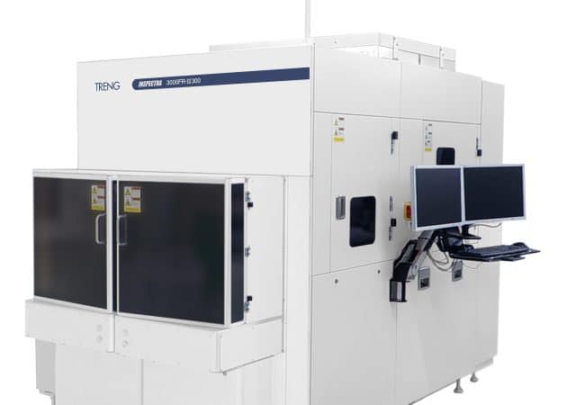
TASMIT Launches Large Glass Substrate Inspection System for Advanced Semiconductor Packaging
TASMIT Inc. has launched a new inspection system for glass substrates as part of its INSPECTRA series of semiconductor wafer visual inspection systems, which has gained attention for its high efficiency in advanced semiconductor manufacturing.
MSTC 2025 to Spotlight Strategies for Bringing MEMS and Sensors Advancements to Market
MEMS and Sensors Technical Congress (MSTC) 2025, the premier technical event on designing, building, and using sensors, will gather industry leaders from across the MEMS and sensors supply chain from March 26-27 at the Georgia Institute of Technology.
Saras Micro Devices Announces Participation in CHIPS National Advanced Packaging Manufacturing Program Initiatives
Saras Micro Devices today announced its participation in two significant projects funded by the U.S. Department of Commerce CHIPS National Advanced Packaging Manufacturing Program (NAPMP).
Terecircuits Becomes National Semiconductor Technology Center Member
Terecircuits Corporation, a venture-backed startup in advanced materials for the semiconductor industry, today announced that it has joined the National Semiconductor Technology Center (NSTC), a public-private consortium established under the CHIPS and Science Act.
Semiconductor Climate Consortium Announces Key 2025 Initiatives
The Semiconductor Climate Consortium (SCC) today unveiled its four key initiatives for 2025, marking a significant step forward in advancing the industry’s commitment to decarbonization and transparency.
indie Semiconductor and GlobalFoundries Announce Strategic Collaboration to Accelerate Automotive Radar Adoption
Silicon, software and proprietary radar system design innovation delivers step-change in radar performance enabling industry’s lowest solution cost or BOM (Bill of Materials) with smallest footprint.
TSMC Intends to Expand Its Investment in the United States to US$165B
Company plans to increase U.S. investment in advanced semiconductor manufacturing by $100 billion with three new fabs, two advanced packaging facilities and an R&D center added to U.S. plans.
Next-Generation AI and Big Data: Transforming Crop Breeding
A new study published in Engineering explores how next-generation artificial intelligence (AI) and big data are revolutionizing crop breeding, with potential far-reaching implications for global food security.
yieldWerx and Incusolution Announce a Strategic Partnership to Strengthen the Presence of the South Korean Semiconductor Industry
yieldWerx, a globally recognized provider of semiconductor yield management solutions, announced a groundbreaking partnership with Incusolution, a semiconductor technology and services firm based in Korea.

