RFMW, a specialized distributor of RF and microwave products, today announced the intention to acquire MRC Gigacomp (MRCG) and MRC Components (MRCC) in Germany.
Leading Edge AI Chipmaker Hailo Introduces Hailo-15
Hailo today announced its groundbreaking new Hailo-15 family of high-performance vision processors, designed for integration directly into intelligent cameras to deliver unprecedented video processing and analytics at the edge.
Boston Semi Equipment Receives Follow-On Order for Multiple High-Voltage Zeus Handlers
Boston Semi Equipment (BSE) today announced that it has received a follow-on order for multiple Zeus gravity handlers for high-voltage device testing.
Draper Opens New Office in Indiana
The office in WestGate@Crane Technology Park will support Microelectronics R&D, strategic programs for the Defense Department and the Naval Surface Warfare Center, Crane Division.
onsemi Commits to the Science Based Targets Initiative
onsemi today announced it has committed to the Science Based Target Initiative (SBTi).
Weebit Nano Partners with University of Florida’s Nino Research Group to Examine Effects of Radiation on Weebit ReRAM
Results of initial studies confirm Weebit ReRAM arrays are tolerant to high radiation levels.
Tokyo Electron Device Joins the Open Invention Network Community
Open Invention Network (OIN), the organization formed to safeguard open source and now the largest patent non-aggression community in history, announced today that Tokyo Electron Device, Ltd. (TED) has joined as a community member
Graphene Quantum Dots Show Promise as Novel Magnetic Field Sensors
Physicists found that speeding electrons trapped in circular loops in graphene quantum dots are highly sensitive to external magnetic fields.
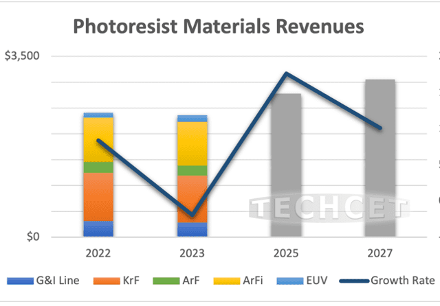
Semiconductor Lithography Materials Trending Upwards
2023 economic slowdown to cause a short-term dip on photoresists & ancillaries.
Alphawave Semi Opens Ottawa Office
Located in the Kanata North technology park, the new office provides more than 20,000 square feet of working space with over 4,000 square feet of laboratory space for its controller, SerDes, and optical engineering teams.