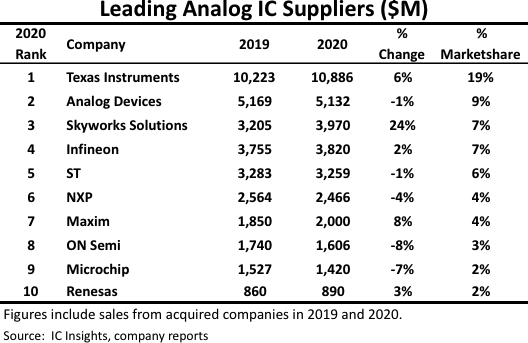
Skyworks Solutions posts strongest sales increase in 2020 as the top-10 suppliers collectively accounted for 62% of total analog sales.
SmartDV Announces Support for ARINC Standards with Design and Verification IP
SmartDV Technologies today announced support of the ARINC standards with its Design and Verification IP.
The Biodegradable Battery
The fabrication device for the battery revolution looks quite unconspicuous: it is a modified, commercially available 3D printer, located in a room in the Empa laboratory building. But the real innovation lies within the recipe for the gelatinous inks this printer can dispense onto a surface.
IEEE International Electron Devices Meeting Announces 2021 Call for Papers
Under the theme “Devices for a New Era of Electronics: From 2D Materials to 3D Architectures,” the 67th annual IEEE International Electron Devices Meeting (IEDM) has issued a Call for Papers seeking the world’s best original work in all areas of microelectronics research and development.
Imec Joins Forces With Sivers Photonics and ASM AMICRA
imec, together with Sivers Photonics and ASM AMICRA Microtechnologies, announced the successful wafer-scale integration of indium-phosphide (InP) distributed feedback (DFB) lasers from Sivers’ InP100 platform onto imec’s silicon photonics platform (iSiPP).
Acorn Technologies Prevails at Trial in Patent Infringement Lawsuit Against Samsung
Acorn Technologies today announced that a jury has found that Samsung Electronics Co., Ltd. infringed all asserted claims of four semiconductor-related patents at a recent trial in the U.S. District Court for the Eastern District of Texas.
Synopsys Expands Multi-Die Solution Leadership with Industry’s Lowest Latency Die-to-Die Controller IP
Synopsys, Inc. today announced its new DesignWare Die-to-Die Controller IP, which complements the company’s existing 112G USR/XSR PHY IP for a complete die-to-die IP solution.
Scientists from NTU and Rice University Uncover Secret Behind One of the World’s Toughest Materials
A team of scientists led by Nanyang Technological University (NTU Singapore) and Rice University in the US, has uncovered the key to the outstanding toughness of hexagonal boron nitride (h-BN).
Dominant Factor of Carrier Transport Mechanism in Multilayer Graphene Nanoribbons Revealed
Researchers precisely set the number of layers in multilayer graphene nanoribbons, controlling the semiconducting and metallic properties of field effect transistors and establishing a design guideline for the practical applications of graphene devices.
Samsung’s Semiconductor Sites Awarded Industry’s First ‘Triple Standard’ by Carbon Trust
All of Samsung’s global semiconductor manufacturing facilities certified for reducing carbon emissions, water use and waste discharge.
