U.S. Sen. Mark R. Warner (D-VA), Vice Chairman of the Senate Select Committee on Intelligence, and Sen. John Cornyn (R-TX) introduced the Creating Helpful Incentives to Produce Semiconductors (CHIPS) for America Act.
NXP Selects TSMC 5nm Process for Next Generation High Performance Automotive Platform
NXP Semiconductors N.V. (NASDAQ: NXPI) and TSMC (TWSE: 2330, NYSE: TSM) today announced a collaboration agreement to adopt TSMC’s 5-nanometer (5nm) technology for NXP’s next generation, high-performance automotive platform.
SEMI Announces Support of CHIPS for America Act to Increase Semiconductor Manufacturing in the U.S.
The bipartisan legislation would improve the competitiveness of semiconductor research, design and manufacturing in the United States, resulting in the creation of thousands of new jobs and bolstering national security.
Minimizing Thermal Conductivity of Crystalline Material with Optimal Nanostructure
Towards application of materials informatics to development of thermal functional materials.
Gartner Forecasts Worldwide Device Shipments to Decline 14% in 2020 Due to Coronavirus Impact
Global shipments of devices (PCs, tablets and mobile phones) are on pace to decline 13.6% in 2020, totaling 1.9 billion units, according to the latest forecast from Gartner, Inc.
Greg Waters joins Mythic Board of Directors
Mythic, an innovative AI inference processor company with breakthrough analog compute-in-memory technology, today announced that Greg Waters has joined the company’s board of directors.
Moortec Launches New In-Chip Technology for Highly Distributed, Real-Time Thermal Analysis on TSMC N5 Process
Moortec today announced an addition to its deeply embedded monitoring portfolio, the Distributed Thermal Sensor (DTS) on TSMC N5 process technology.
Deep Learning Robotics Granted New Patent from U.S. Patent Office for Robotic Learning
Deep Learning Robotics Ltd., a leading technology company focused on robotics and automation solutions, announced that the United States Patent and Trademark Office has granted the company a new patent, No. US10,571,896.
Crystalline ‘Nanobrush’ Clears Way to Advanced Energy and Information Tech
A team led by the Department of Energy’s Oak Ridge National Laboratory synthesized a tiny structure with high surface area and discovered how its unique architecture drives ions across interfaces to transport energy or information. Their “nanobrush” contains bristles made of alternating crystal sheets with vertically aligned interfaces and plentiful pores.
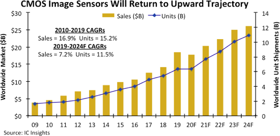
CMOS Image Sensors to Resume Record Run in 2021
The fallout from the Covid-19 virus crisis in 2020 is expected to lower CMOS image sensor sales for the first time in 10 years, but new record-high revenues are seen next year, says new O-S-D Report.
