Deep Learning Robotics Ltd., a leading technology company focused on robotics and automation solutions, announced that the United States Patent and Trademark Office has granted the company a new patent, No. US10,571,896.
Crystalline ‘Nanobrush’ Clears Way to Advanced Energy and Information Tech
A team led by the Department of Energy’s Oak Ridge National Laboratory synthesized a tiny structure with high surface area and discovered how its unique architecture drives ions across interfaces to transport energy or information. Their “nanobrush” contains bristles made of alternating crystal sheets with vertically aligned interfaces and plentiful pores.
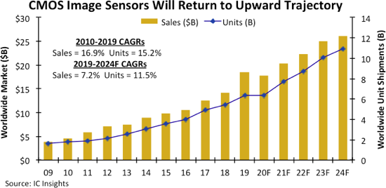
CMOS Image Sensors to Resume Record Run in 2021
The fallout from the Covid-19 virus crisis in 2020 is expected to lower CMOS image sensor sales for the first time in 10 years, but new record-high revenues are seen next year, says new O-S-D Report.
Synopsys Acquires Semiconductor Analytics Innovator Qualtera
Synopsys, Inc. (NASDAQ: SNPS) today announced it has acquired Qualtera, a fast-growing provider of collaborative high-performance, big data analytics for semiconductor test and manufacturing.
Mitsubishi Electric to Acquire Factory to Expand Power Device Business
Mitsubishi Electric Corporation (TOKYO: 6503) announced today that it will acquire buildings and land from Sharp Fukuyama Semiconductor Co., Ltd., a wholly owned subsidiary of Sharp Corporation located in Fukuyama, Hiroshima Prefecture, Japan.
Samsung Receives Zero Waste to Landfill Validations for All of its Global Semiconductor Manufacturing Sites
Samsung Electronics Co., Ltd., a world leader in advanced semiconductor technology, today announced that it has received UL’s Zero Waste to Landfill validation of Gold level and above for all of its global semiconductor operation sites.
Flexible and Recyclable Optoelectronics Move a Step Closer
Australian researchers have demonstrated the strong potential for a new type of flexible, recyclable electrodes to be used in creating cheaper solar cells, touchscreens, wearable ‘e-skins’ and next-generation responsive windows.
CEA-Leti Researchers Break Throughput Record for LiFi Communications Using Single GaN Blue Micro-Light-Emitting Diode
CEA-Leti today announced its researchers have broken the throughput world record of 5.1 Gbps in visible light communications (VLC) using a single GaN blue micro- light-emitting diode (LED).
COVID-19 Triggers Accelerated Shift to Digital Technologies and Services
The ongoing digital transformation of business and society has been shifted into overdrive by the COVID-19 pandemic, triggering major changes in key segments ranging from online services, to capital spending, to the cloud, to the electronics supply chain.
Paragraf Partners with CERN to Demonstrate Unique Properties of Paragraf’s New Graphene Hall Effect Sensor
Paragraf has embarked on a working partnership with the Magnetic Measurement section at CERN, the European Organization for Nuclear Research, to demonstrate how new opportunities for magnetic measurements are opened up through the unique properties of its graphene sensor, particularly its negligible planar Hall effect.
