It was a year when global semiconductor revenue fell by the greatest percentage in at least two decades, when eight of the top-10 chip suppliers suffered revenue declines and when sales fell for every application market and for every global region. The year 2019 was also the time when Intel bucked the trend—achieving growth and reclaiming the market’s top spot as the company’s long-term diversification strategy paid dividends during a challenging period for the semiconductor business, according to Omdia.
Global Semiconductor Materials Market Revenues Slip 1.1 Percent in 2019, SEMI Reports
Global semiconductor materials market revenues edged down 1.1 percent in 2019, SEMI, the global industry association representing the electronics manufacturing and design supply chain, reported today in its Materials Market Data Subscription (MMDS). While worldwide total wafer fabrication materials logged a slight decrease of 0.4 percent, from $33.0 billion to $32.8 billion, wafer fab materials, process chemicals, sputtering targets, and CMP registered declines of more than 2 percent year-over-year.
SEMI Urges ‘Essential Business’ Designation of Semiconductor Companies Worldwide to Help Ensure Continuous Operation
SEMI has urged government representatives around the U.S. and world to designate the semiconductor industry as an essential business so operations at companies across the chip supply chain can continue without interruption as the spread of COVID-19 continues. SEMI President and CEO Ajit Manocha assured the U.S. and global officials that SEMI members – the device makers and suppliers of chemicals, materials, components, design tools and equipment at the heart of chip manufacturing – “are employing all measures necessary to maintain the health and safety of their employees and local communities” to help contain the virus.
Intel Allocates $6M to Coronavirus Relief
The Intel Foundation will provide $4 million to support coronavirus relief efforts in communities where the company has significant presence. The foundation will also offer a special match opportunity for every regular full-time and part-time employee and U.S. retiree to a total of $2 million for relief efforts around major Intel sites.
miDiagnostics Raises €14m to Accelerate the Commercialization of its Disruptive, Lab-quality Silicon Chip Diagnostics Platform
miDiagnostics, which is using silicon chip technology that will bring miniaturized, rapid, easy-to-use, lab-quality tests with built-in connectivity direct to the patient and clinician regardless of location, today announces the completion of a €14m investment round. This technology has potential to deliver rapid test results in multiple settings, including future pandemics.
MagnaChip Semiconductor Announces Definitive Agreement To Sell Foundry Business and Fab 4
MagnaChip Semiconductor Corporation today announced that certain of its wholly-owned subsidiaries have entered into a definitive agreement to sell the Company’s Foundry Services Group and the factory in Cheongju, the larger of the Company’s two 8″ manufacturing facilities, to a special purpose company in South Korea established by Alchemist Capital Partners Korea Co., Ltd. and Credian Partners, Inc.
New Case Study from Cobham Advanced Electronic Solutions Touts Everspin’s Toggle MRAM as a Highly Reliable Memory Technology for Space Applications
Everspin Technologies, Inc.‘s (NASDAQ: MRAM) partner Cobham Advanced Electronic Solutions (CAES) recently presented a technical case study describing the versatility and performance of their jointly developed Toggle MRAM for space applications.
Nordson Corporation Announces Business Realignment and Leadership Appointments
Nordson Corporation (Nasdaq: NDSN) today announced a strategic business realignment that will position the company for its next chapter of profitable growth. The company will reorganize into two businesses: Industrial Precision Solutions (IPS) led by Gregory P. Merk, Executive Vice President, and Advanced Technology Solutions (ATS) led by Jeffrey A. Pembroke, Executive Vice President.
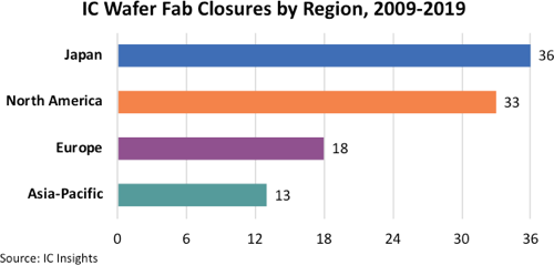
100 IC Wafer Fabs Closed or Repurposed Since 2009
Hardest hit are ≤200mm wafer fabs; 70% of closures in Japan and North America.
Toshiba’s 80V N-channel Power MOSFETs Fabricated with Latest Generation Process Help Improve Power Supply Efficiency
Toshiba Electronic Devices & Storage Corporation (“Toshiba”) has added 80V N-channel power MOSFETs to its “U-MOS X-H series” fabricated with the latest generation process. The new MOSFETs are suitable for switching power supplies in industrial equipment used in data centers and communication base stations.

