The recent surge of the spread of the coronavirus (Covid-19) and its anticipated negative impact on the global economy and IC market definitely fits the definition of a Black Swan event.
Fish Scales Could Make Wearable Electronics More Sustainable
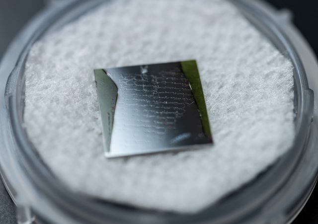
Flexible temporary electronic displays may one day make it possible to sport a glowing tattoo or check a reading, like that of a stopwatch, directly on the skin. In its current form, however, this technology generally depends on plastic. New research in ACS Nano describes a way to make these displays, which would likely be discarded after a single use, more environmentally friendly using a plentiful and biodegradable resource: fish scales.
Power Integrations’ SCALE-iDriver for SiC MOSFETs Achieves AEC-Q100 Automotive Qualification
Power Integrations (Nasdaq: POWI), the leader in gate-driver technology for medium- and high-voltage inverter applications, today announced that its SIC118xKQ SCALE-iDriver™, a high-efficiency, single-channel gate driver for silicon carbide (SiC) MOSFETs, is now certified to AEC-Q100 for automotive use. Devices can be configured to support gate-drive voltage requirements of commonly used SiC MOSFETs and feature sophisticated safety and protection features.
CyberOptics Receives New Orders for Memory Module and Micro LED Inspection and Metrology Systems
CyberOptics Corporation® (Nasdaq: CYBE), a leading global developer and manufacturer of high precision 3D sensing technology solutions, today announced that it has received orders valued at approximately $2.8 million for its 2D MX600™ system for post-singulation inspection of memory modules. CyberOptics presently anticipates that these orders will become revenue in the third quarter of 2020.
Semiconductors Can Behave Like Metals and Even Like Superconductors
The crystal structure at the surface of semiconductor materials can make them behave like metals and even like superconductors, a joint Swansea/Rostock research team has shown. The discovery potentially opens the door to advances like more energy-efficient electronic devices. Semiconductors are the active parts of transistors, integrated circuits, sensors, and LEDs. These materials, mostly based on silicon, are at the heart of today’s electronics industry.
Novel Approach to Enhance Performance of Graphitic Carbon Nitride
In a report published in NANO, scientists from the Jiangxi University of Science and Technology, Guangdong University of Petrochemical technology, Gannan Medical University and Nanchang Hangkong University in China underline the importance of defect engineering to promote catalytic performance by providing a simple and efficient way for modifying and optimizing metal-free semiconductor photocatalyst graphitic carbon nitride (g-C3N4) to solve the dual problems of environmental pollution and lack of fossil resources.
Ferdinand-Braun-Institut Chooses Solstice S4 for Advanced Electroplating and Wafer Surface Processing
ClassOne Technology, global supplier of advanced electroplating systems for ≤200mm wafer processing, announced the sale of its Solstice® S4 system to the Ferdinand-Braun-Institut (FBH) in Berlin. The FBH is a major III-V compound semiconductor research institute that develops leading-edge microwave and optoelectronic devices for communications, energy, health, mobility and other industries.
New SEMI Job Skills Model for Growing Microelectronics Industry Talent Pipeline Released by U.S. Department of Labor – Employment and Training Administration
SEMI today announced the release of a central feature of its workforce development initiative, designed to grow the microelectronics industry’s talent pipeline, on the U.S. Department of Labor’s Competency Model Clearinghouse website. The Unified Competency Model (UCM) for Advanced Manufacturing identifies skill sets required across strategic industry sectors to strengthen connections among the microelectronics industry, workers, and education and training providers.
OnScale is Providing Free Cloud Core-Hours to Customers to Mitigate Engineering Productivity Loss Related to the Coronavirus Outbreak
OnScale, the global leader in Cloud Engineering Simulation, today announces that it will provide free cloud core-hours to customers to promote customer safety and mitigate any productivity loss due to office shutdowns. OnScale has already officially closed its global offices to protect the health and safety of OnScale employees.
Room-temperature Bonded Interface Improves Cooling of Gallium Nitride Devices
A room-temperature bonding technique for integrating wide bandgap materials such as gallium nitride (GaN) with thermally conducting materials such as diamond could boost the cooling effect on GaN devices and facilitate better performance through higher power levels, longer device lifetime, improved reliability, and reduced manufacturing costs.

