Compound Photonics US Corporation (CP), a leading provider of compact high-resolution microdisplay solutions for Augmented Reality (AR) and Mixed Reality (MR) applications, and Plessey Semiconductors Ltd. (Plessey), an embedded technologies developer at the forefront of microLED technology for AR and MR display applications, today announced they have produced the first fully addressable microLED display modules resulting from their previously announced strategic partnership to develop and introduce GaN-on-Silicon microLED based microdisplay solutions for AR/MR applications.
‘Atomic Dance’ Reveals New Insights Into Performance of 2D Materials
A team of Northwestern University materials science researchers have developed a new method to view the dynamic motion of atoms in atomically thin 2D materials. The imaging technique, which reveals the underlying cause behind the performance failure of a widely used 2D material, could help researchers develop more stable and reliable materials for future wearables and flexible electronic devices.
Nanowires Made of Tellurium and Nanotubes Hold Promise for Wearable Tech
Wearable tech and electronic cloth may be the way of the future, but to get there the wiring needs to be strong, flexible and efficient. Boron nitride nanotubes (BNNT), studied by physicists at Michigan Technological University, encase tellurium atomic chains like a straw, which could be controllable by light and pressure. In collaboration with researchers from Purdue University, Washington University and University of Texas at Dallas, the team published their findings in Nature Electronics this week.
Emerging Market for Low-Density Panel FO Analyzed
Large area fan-out (FO) remains a hot topic in the industry. There is some confusion over the term “panel” because IC package substrates are processed in panels. The main driver for large area FO panel development is cost reduction because more parts can be processed in a batch. TechSearch International’s latest Advanced Packaging Update report divides the panel market into high-density RDL (≤2μm L/S with multiple RDLs) versus low-density (>5μm L/S with ≤3 RDLs).
SEMI President and CEO Ajit Manocha Set for Induction into Silicon Valley Engineering Hall of Fame
Semiconductor industry veteran and SEMI president and CEO Ajit Manocha will be inducted into the Silicon Valley Engineering Hall of Fame on February 19, 2020. The Silicon Valley Engineering Council (SVEC) is honoring Manocha for championing industry collaboration and driving manufacturing efficiency in multiple leadership roles, as well as for his work as one of the pioneers of reactive ion etching and manufacturing process flows for logic and memory chips that serve as the foundation for modern microelectronics manufacturing.
MKS Announces Series 49UL Thermal Management System
The Series 49UL Thermal Management System with improved heater diagnostics capability and UL and CE safety certifications creates continuous heater monitoring and status, ensuring manufacturing process safety. With heater jackets made of high quality Polyimide or Polytetrafluoroethylene (PTFE), the S49UL provides high temperature operation and uniformity while being light weight and flexible for easy installation.
Autotalks’ Chipset is Selected for the Company’s First Mass Production C-V2X Program in China
Autotalks, a world leader in V2X (Vehicle-to-Everything) communication solutions, announced that its chipset was selected for a mass production C-V2X program in China, one of the first to be deployed in the huge Chinese market. This is the first mass-production C-V2X program for Autotalks, which consists of a Telematics Control Unit (TCU) with C-V2X powered by Autotalks’ chipset, built by a top Tier1 automotive provider.
2020 IEEE International Reliability Physics Symposium to Highlight Latest Research in Reliability for Semiconductor Devices, Microelectronic Systems, and Advanced Technologies
The upcoming 2020 IEEE International Reliability Physics Symposium (IRPS), the industry’s premier technical conference for engineers and scientists to present the latest original research in microelectronics reliability, will be held in Dallas, TX from March 29 – April 2, 2020 at the Hilton DFW Lakes Executive Conference Center. The Symposium will feature a number of special focus sessions highlighting novel and emerging areas of electronic reliability, as well as topics relating to conventional semiconductor, integrated circuit, and microelectronic assembly reliability.
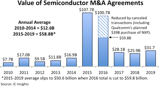
Acquisition Rebound Lifts 2019 to Third-Largest M&A Year
Seven major semiconductor acquisition agreements valued at $1 billion or more increase the total value of all deals by 22% from the previous year, continuing the strong wave of M&A and consolidation among chip suppliers.
SemiQ Announces Next Generation 650V, 1200V, and 1700V Silicon Carbide Schottky Diode Family
SemiQ (previously Global Power Technologies Group) recently announced the release to production of its new 3rd generation SiC Diode Family featuring blocking voltages of 650V, 1200V and 1700V with forward-current starting at 8 amps up to 50 A per chip. Packages include TO-220-2L, TO-220-3L, TO-247-2L, TO-247-3L, SOT-227, TO-263 as well as bare die.
