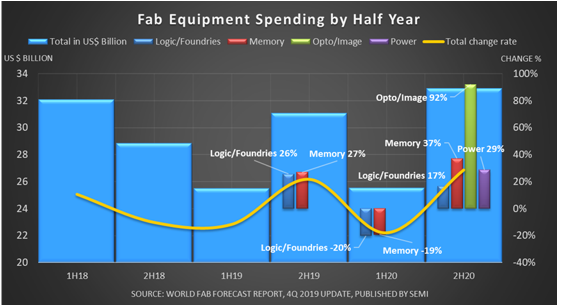
Projected 2019 global fab equipment spending has been revised upward to US$56.6 billion on the strength of surging memory investments in the latter part of the year after a weak first half, SEMI reported today in its World Fab Forecast. SEMI data now point to just a 7 percent decline in fab equipment investments from 2018 to 2019, a marked improvement on the previously forecast drop of 18 percent. Rising investments in memory – particularly 3D NAND – leading-edge logic and foundries have powered the turnaround.
FLEX and MSTC 2020 to Showcase Flexible Hybrid Electronics, MEMS and Sensors Innovations for More Personalized Applications
Flexible hybrid electronics breakthroughs are driving the next wave of smart MEMS and sensing solutions for more personalized, portable electronics, setting the stage for the co-located Flexible Hybrid Electronics Conference and Exhibition (FLEX) and MEMS & Sensors Technical Congress (MSTC) Feb. 24-27, 2020. Co-sponsored by SEMI FlexTech and SEMI MEMS & Sensors Industry Group, FLEX and MSTC will gather more than 100 global experts for market and technical presentations, tech courses, and more than 50 exhibit opportunities for connecting with industry visionaries at the DoubleTree by Hilton Hotel in San Jose, Calif. Registration is now open.
MIRISE Technologies to be Launched to Develop Semiconductors in Effort to Achieve Safe and Comfortable Future Global Mobility Society
DENSO Corporation and Toyota Motor Corporation today announced that they have named the joint venture to be established in April 2020 MIRISE Technologies (“MIRISE”). The joint venture will conduct research and advanced development of next-generation in-vehicle semiconductors. MIRISE is an acronym for Mobility Innovative Research Institute for SEmiconductors. It also conveys “mirai” (a Japanese word for “future”) and “rise.” Yoshifumi Kato has been appointed President and Representative Director of the new company.
Industry Veteran Dr. Randy Allen Joins SiFive as Vice President of RISC-V Software
SiFive, Inc., the leading provider of commercial RISC-V processor IP and silicon solutions, today announced that Dr. Randy Allen has joined the company as vice president of RISC-V software. Dr. Allen will be responsible for developing and implementing RISC-V software strategy for SiFive. Dr. Allen brings more than 30 years of industry experience and, most recently, served as vice president of software engineering at Wave Computing. He has also served in leadership roles at tech companies such as Mentor Graphics, National Instruments and Cypress Semiconductor.
QuickLogic Names New Chairman of the Board
QuickLogic Corporation (NASDAQ: QUIK), a developer of ultra-low power multi-core voice-enabled SoCs, embedded FPGA IP, and Endpoint AI solutions, today announced the appointment of Michael R. Farese as the Chairman of the Board of Directors, effective December 6, 2019 to replace E. Thomas Hart, who passed away on December 3, 2019. Michael R. Farese (Ph.D.) has been serving as a member of QuickLogic’s Board of Directors since April 2008, most recently as the lead independent director, and brings to the position a deep understanding of consumer products, converged devices and wireless markets.
Aldec’s New FPGA-based NVMe Data Storage Solution Targets High Performance Computing Applications
Aldec, Inc., a pioneer in mixed HDL language simulation and hardware-assisted verification for FPGA and ASIC designs, has launched a powerful, versatile and time- saving FPGA-based NVMe Data Storage solution to aid in the development of High Performance Computing (HPC) applications such as High Frequency Trading and Machine Learning. The solution includes an Aldec TySOM embedded prototyping board, up to eight high-bandwidth, low- latency FMC-NVMe daughter cards, and a reference design (including source files and binaries) allowing engineers to fast-track their projects.
Nordson Corporation Announces Planned Retirement of Chief Financial Officer
Nordson Corporation (NASDAQ-NDSN) today announced that Gregory A. Thaxton, Executive Vice President and Chief Financial Officer, plans to retire in 2020 after thirty successful years with the company, with the last 12 years as CFO. The company has initiated a search of internal and external candidates for his successor. Mr. Thaxton will remain in his current role throughout this transition period. Mr. Thaxton started his career with Nordson in 1989. He became part of the executive leadership team in February 2007 when he was named Corporate Controller and Chief Accounting Officer. He was appointed CFO in January 2008.
Universal Display Corporation Announces the Appointment of New Board Members
Universal Display Corporation (Nasdaq: OLED), enabling energy-efficient displays and lighting with its UniversalPHOLED technology and materials, today announced that Cynthia J. Comparin and Celia M. Joseph have been appointed as independent members to its Board of Directors, effective January 1, 2020. These new additions will expand Universal Display’s board to 9 members. Cynthia Comparin brings approximately 30 years of leadership experience in international business, financial and strategic planning. Celia Joseph brings approximately 40 years of leadership experience in global human resource management and law.
Tiny Quantum Sensors Watch Materials Transform Under Pressure
Since their invention more than 60 years ago, diamond anvil cells have made it possible for scientists to recreate extreme phenomena – such as the crushing pressures deep inside the Earth’s mantle – or to enable chemical reactions that can only be triggered by intense pressure, all within the confines of a laboratory apparatus that you can safely hold in the palm of your hand. To develop new, high-performance materials, scientists need to understand how useful properties, such as magnetism and strength, change under such harsh conditions. But often, measuring these properties with enough sensitivity requires a sensor that can withstand the crushing forces inside a diamond anvil cell.
ULVAC Inc. and Silex Microsystems AB Sign Joint Development Agreement on Leading-Edge Sputtered PZT for MEMS
ULVAC, Inc. (ULVAC), headquartered in Kanagawa, Japan and lead by CEO Setsuo Iwashita and SILEX Microsystems AB (Silex), headquartered in Järfälla, Sweden and lead by CEO Edvard Kälvesten, today announced they have signed an agreement to develop a production thin film piezoelectric process (PZT) for MEMS actuators and sensors with cutting edge performance and reliability.