In a research result that potentially could expand the market for tiny energy-storage units in medical implantable, injectable and wearable solutions, CEA-Leti has fabricated all-solid, inorganic thin-film batteries (TFBs) that demonstrate better performance than existing devices. During its presentation at IEDM 2019, a CEA-Leti team reported that, “Thin-film batteries provide some of the highest energy densities of electrochemical energy storage devices, but the inability to increase the electrodes’ thicknesses and control the geometry on the micrometer scale has thus far hindered their effective areal energy density and integration in miniaturized devices.”
Global Semiconductor Equipment Sales Forecast – 2020 Rebound, 2021 Record High
Global semiconductor manufacturing equipment sales will drop 10.5 percent to $57.6 billion in 2019 from last year’s historic peak of $64.4 billion but stage a 2020 recovery and set a new high in 2021, SEMI, the global industry association representing the electronics manufacturing and design supply chain, reported today in its Year-End Total Equipment Forecast. Released at SEMICON Japan 2019, the forecast shows equipment sales registering a 5.5 percent increase to $60.8 billion in 2020 and continued expansion into 2021, with record revenues of $66.8 billion as leading device manufactures invest in sub-10nm equipment, especially for foundry and logic.
MIPT Researchers Close In On New Nonvolatile Memory
Researchers from the Moscow Institute of Physics and Technology, along with their colleagues from Germany and the U.S., have achieved a breakthrough on the way to new types of nonvolatile memory devices. The team came up with a unique method for measuring the electric potential distribution across a ferroelectric capacitor — the device underlying the memory of the future, which would be orders of magnitude faster than the current flash and solid-state drives, withstanding 1 million times as many rewrite cycles. The paper was published in Nanoscale.
SEMICON Japan 2019 Opens Tomorrow: SMART Transportation, SMART Manufacturing and Business Continuity Planning in Focus
SEMICON Japan 2019, the largest and most influential gathering of the electronics manufacturing supply chain in Japan with nearly 55,000 attendees expected, opens tomorrow at Tokyo Big Sight to focus on growth opportunities in smart transportation and smart manufacturing and the critical importance of business continuity planning (BCP). Industry leaders and visionaries from across the electronics supply chain will gather December 11-13 at SEMICON Japan 2019 – themed Enabling a Smarter World – for insights into the latest technologies, innovations and trends in the electronics industry.
Breker Verification Systems Launches Unique RISC-V TrekApp for Automated, High-Coverage System Integration Test Suite Synthesis
Breker Verification Systems, the provider of Test Suite Synthesis tools based on the Portable Stimulus Standard (PSS), today introduced its RISC-V TrekApp, a complete, automated test content generator for RISC-V system integration testing. RISC-V TrekApp, the first solution to address the entire RISC-V system-on-chip (SoC) system integration problem, targets complex verification challenges and increases coverage by executing unpredictable corner-case scenarios without the need for manually developed test content. The TrekApp works with existing universal verification methodology (UVM) and SoC verification environments and does not require the user to learn the PSS language.
Imec Presents Forksheet Device as The Ultimate Solution to Push Scaling Towards the 2nm Technology Node
This week, at the 2019 IEEE International Electron Devices Meeting, imec, a world-leading research and innovation hub in nanoelectronics and digital technologies, presents first standard cell simulation results of its forksheet device designed for sub-3nm logic technology nodes. Compared to nanosheet devices, the reduced n-to-p spacing results in a 10 percent performance increase. When combined with scaling boosters, the new device architecture will bring logic standard cell height down to 4.3 tracks, which combined with cell template optimization can result in more than 20 percent area reduction. The results value the forksheet architecture as a potential solution to extend the scalability of nanosheet structures beyond the 3nm logic technology node.
NSITEXE Selects SmartDV TileLink Verification IP for RISC-V Based Applications
SmartDV™ Technologies today announced NSITEXE licensed its TileLink VIP to ensure complete verification of its high-efficiency and high-quality semiconductor IP adaptable to various applications using the RISC-V architecture. NSITEXE selected SmartDV because it is the only VIP solutions provider to offer a smart way to verify the TileLink fabric and reduce verification time. SmartDV’s VIP verifies the TileLink chip-scale interconnect standard, an open-source, high-performance and scalable cache-coherent fabric for RISC-V based or alternative architecture system-on-chip (SoC) designs.
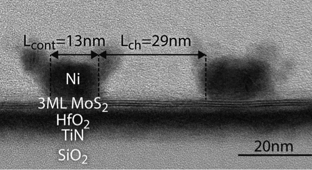
Imec Shows Excellent Performance in Ultra-Scaled FETs with 2D-Material Channel
At this year’s IEEE International Electron Devices Meeting (Dec 7-11 2019), imec, a world-leading research and innovation hub in nanoelectronics and digital technologies, reports an in-depth study of scaled transistors with MoS2 and demonstrates best device performance to date for such materials.
Creating Switchable Plasmons in Plastics
Researchers in the Organic Photonics and Nano-optics goup at the Laboratory of Organic Electronics have developed optical nanoantennas made from a conducting polymer. The antennas can be switched on and off, and will make possible a completely new type of controllable nano-optical components.
memsstar Ships MEMS Production System to University of Freiburg in Support of the PROMYS Project
memsstar Ltd., a provider of etch and deposition equipment to manufacturers of semiconductors and microelectrical mechanical systems (MEMS), announced today shipment of its three-chamber ORBIS™ 3000 system for MEMS research and manufacturing to the Department of Microsystems Engineering (IMTEK) at the University of Freiburg, Germany. As part of the nationally funded project, “Processes and Materials for More-than-Moore Electronic Systems (PROMYS),” memsstar’s surface micromachining cluster tool will serve as a central unit for the micromechanical structuring of MEMS components for up to 200mm wafers.