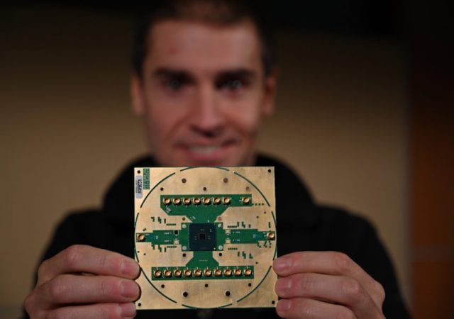
Intel Labs today unveiled what is believed to be a first-of-its-kind cryogenic control chip — code-named “Horse Ridge” — that will speed up development of full-stack quantum computing systems.
SiFive Retains Title of Most Respected Private Semiconductor Company
SiFive, the leading provider of commercial RISC-V processor IP and silicon solutions, today announced it has been recognized for the second consecutive year as the Most Respected Private Semiconductor Company by the Global Semiconductor Alliance (GSA) at the GSA Awards Dinner on Dec. 5, 2019. This recognition tops a milestone year for the company, which announced more than 130 design wins, completed Series D investments to secure over $100M total funding to date and continued to attract the industry’s top talent.
Analog Devices Files Patent Infringement Lawsuit Against Xilinx
Analog Devices, Inc. (Nasdaq: ADI), a leading global high-performance analog technology company, today announced that it has filed a patent infringement lawsuit against Xilinx, Inc. (Nasdaq: XLNX). The lawsuit focuses on the unauthorized use by Xilinx of several important ADI patents relating to converter technology in at least two of Xilinx’s High End Zynq UltraScale+ RFSoC products.
Global Semiconductor Alliance Announces 2019 GSA Award Recipients
The Global Semiconductor Alliance (GSA) is proud to announce the award recipients honored at the 2019 GSA Awards Dinner Celebration that took place last evening in Santa Clara, Calif. For a quarter century, the GSA Awards have recognized the achievements of top performing semiconductor companies in several categories ranging from outstanding leadership to financial accomplishments, as well as overall respect within the industry.
Keysight, Marvin Test Solutions Collaborate to Speed Manufacturing of mmWave Semiconductors
Keysight Technologies, Inc. (NYSE: KEYS), a technology company that helps enterprises, service providers and governments accelerate innovation to connect and secure the world, announced that its collaboration with Marvin Test Solutions, Inc. (MTS) – a supplier of functional test solutions – has resulted in the development of a fast and accurate 5G semiconductor manufacturing test platform. The two parties focused on advancing beamformer integrated circuit (IC) test technology to help manufacturers of semiconductors accelerate the production of high performance 5G integrated ICs. Marvin – a trusted provider of globally-deployed test solutions for military, aerospace, and manufacturing organizations – integrated Keysight’s PXIe-based Vector Network Analyzer (VNA) to achieve accurate and fast measurements in its TS-960e-5G mmWave Test System.
Scientists See Defects in Potential New Semiconductor
A research team has reported seeing, for the first time, atomic scale defects that dictate the properties of a new and powerful semiconductor. The study, published earlier this month in the journal Physical Review X, shows a fundamental aspect of how the semiconductor, beta gallium oxide, controls electricity. Scientists have known about beta gallium oxide for about 50 years, but only in the last several years has it become an intriguing option for engineers looking to build more reliable, more efficient high-powered technologies. The material is especially well-suited for devices used in extreme conditions, such as in the defense industry. The team has been studying beta gallium oxide for its potential to provide high-density power.
Weebit Nano and Leti File Three New Patents for Improved Yield and Reliability of Advanced ReRAM Products
Weebit Nano (ASX: WBT), the next generation memory technology for the global semiconductor industry, and its development partner Leti, the French research institute recognised as a global leader in the field of micro-electronics, have filed three new patents for Weebit’s Silicon Oxide (SiOx) ReRAM
technology. The latest patents from Weebit and Leti use newly developed smart algorithms to increase the reliability and yield of ReRAM memory cells and enable scalable immune ReRAM process improvements. Two patents identify failure modes, in which optimised smart programming algorithms then improve the window margin and array yield. The third patent improves process flows, allowing increased stability at scaled memory cells in geometries of 40nm and below.
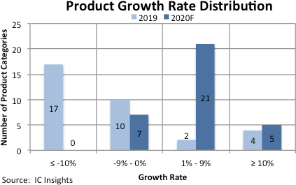
NAND Flash to Lead All Others As IC Market Growth Returns in 2020
IC Insights is in the process of revising its forecast and analysis of the IC industry and will present its new findings in The McClean Report 2020, which will be released in January 2020. Among the revisions is a complete update of forecast growth rates of the 33 main product categories classified by the World Semiconductor Trade Statistics organization (WSTS) through the year 2024. The top five categories for IC product growth are covered in this bulletin.
OneSpin Addresses the Challenges of RISC-V Verification at the Annual RISC-V Summit
OneSpin Solutions, provider of certified IC integrity verification solutions for building functionally correct, safe, secure, and trusted integrated circuits, will showcase its verification expertise of RISC-V processor cores at the upcoming RISC-V Summit being held December 10-12, 2019 at the San Jose Convention Center. OneSpin will host attendees at both its booth and a demo pod in the OpenHW pavilion at the RISC-V Summit, while the company’s experts will present two sessions on verifying RISC-V SoCs.
IEDM’s Monday is MRAM Day – Part 2
Samsung gives a second paper this session, detailing (2.5) A Novel Integration of STT-MRAM for On-chip Hybrid Memory by Utilizing Non-Volatility Modulation, with Jeong-Heon Park as lead author. “We demonstrate a novel way of integrating STT-MRAM for on-chip hybrid memory which exhibits either features of high-retention or high-speed implemented in separate zones in a single chip. For satisfying high temperature retention requirement, tailored MTJs are shown to support >10-year retention at 220℃.” MRAM switching protocols can be tuned for either high speed or high retention, so here we have a process which gives the option of both on the same die.