Researchers at Nanyang Technological University, Singapore (NTU Singapore) have developed a quantum communication chip that is 1,000 times smaller than current quantum setups, but offers the same superior security quantum technology is known for. Roughly 3mm in size, the tiny chip developed by NTU scientists uses quantum communication algorithms to provide enhanced security compared to existing standards. It does this by integrating passwords within the information that is being delivered, forming a secure ‘quantum key’. After the information is received, it is destroyed along with the key, making it an extremely secure form of communication.
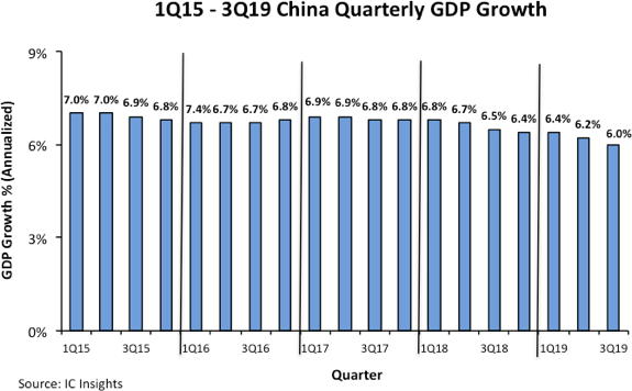
China GDP and PMI Contraction A Risk Factor For Global Economy
IC Insights recently released its October Update to The McClean Report 2019. Part of the update reviewed U.S. and China GDP and PMI trends in light of the current trade friction between the two nations.
GLOBALFOUNDRIES and TSMC Announce Resolution of Global Disputes Through Broad Global Patent Cross-License
GLOBALFOUNDRIES (GF) and TSMC today announced they are dismissing all litigation between them as well as those that involve any of their customers. The companies have agreed to a broad life-of-patents cross-license to each other’s worldwide existing semiconductor patents as well as those patents that will be filed during the next ten years as both companies continue to invest significantly in semiconductor research and development. This resolution guarantees GF and TSMC freedom to operate and ensures that their respective customers will continue to have access to each foundry’s complete array of technologies and services.
James C. Morgan, Chairman Emeritus of Applied Materials, Inc., Awarded the Global Semiconductor Alliance’s Premier Accolade
The Global Semiconductor Alliance (GSA) will honor James (“Jim”) C. Morgan, Chairman Emeritus of Applied Materials, Inc., with the esteemed Dr. Morris Chang Exemplary Leadership Award at its highly-anticipated Annual Awards Dinner to be held in Santa Clara, Calif., on Dec. 5, 2019. Morgan is an industry leader and visionary who led Applied Materials for nearly three decades — one of the longest tenures of a Fortune 500 CEO. He served as CEO from 1977 to 2003 and chairman of the board from 1987 to 2009, growing Applied from less than $20 million to more than $9 billion in revenue during that time.
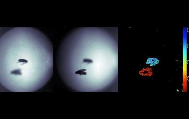
Compact Depth Sensor Inspired By Spiders
For all our technological advances, nothing beats evolution when it comes to research and development. Take jumping spiders. These small arachnids have impressive depth perception despite their tiny brains, allowing them to accurately pounce on unsuspecting targets from several body lengths away.
Study Shows Ability to Detect Light From UV to the IR Optical Regimes Using Spin Currents
A University of Wyoming researcher and his team have shown that the spin Seebeck effect (SSE) can be used to detect light across a broad optical range – ultraviolet through visible to near-infrared. This work has future implications on novel spin current-based technologies. The SSE is one of three known ways to generate spin current, or a net movement of particle magnet moments. The SSE occurs when a thermal gradient is created across a material and, depending on how it is measured, results in an electrical potential. However, unlike its electrical analog, the SSE has been generated not just in ferromagnetic metals – such as cobalt, iron and nickel — and semiconductors, but also in magnetic insulators, making it widely applicable.
AKHAN Announces Major Patents Issued for Diamond Semiconductor Optics & Electronics Applications by US and Japan Patent Offices
AKHAN Semiconductor, a technology company specializing in the fabrication and application of lab-grown, electronics-grade diamond, announced today issuances by both the United States Patent and Trademark Office (USPTO) and Japan Patent Office (JPO) of patents covering AKHAN’s next-generation n-type diamond semiconductor system and diamond-based multilayer antireflective coating systems, key in military & aerospace sensor and detector applications, amongst others. The granted and issued patents, 6580644 in Japan and 10,422,928 & 10,410,860 in the US, are key additions to AKHAN’s breakthrough Miraj Diamond® intellectual property portfolio, and enable breakthrough performance in semiconductor devices as well as new capabilities in optical sensing, detecting, and transmission.
David Zinsner Appointed to Credo Board of Directors
Credo, a global innovation leader in Serializer-Deserializer (SerDes) technology which delivers high performance, low power connectivity solutions for 100G, 400G, and 800G port enabled networks, today announced the appointment of David Zinsner to Credo’s Board of Directors. He is currently Senior Vice President and Chief Financial Officer at Micron Technology, Inc. (Nasdaq: MU). Zinsner joined Micron in February 2018 with more than 20 years of financial and operations experience in the semiconductor and technology industry, after serving as President and Chief Operating Officer at Affirmed Networks. Previously, he was Senior Vice President of Finance and Chief Financial Officer at Analog Devices.
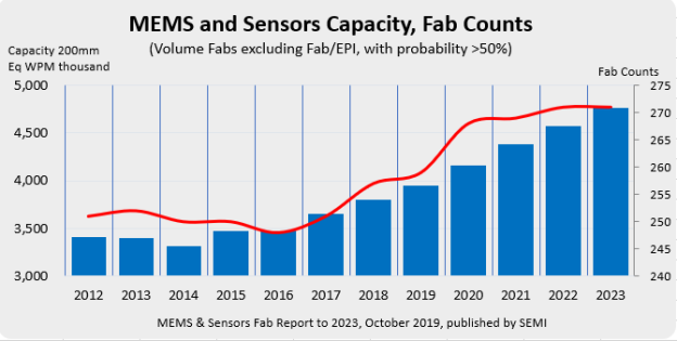
Global MEMS and Sensors Fab Capacity to Grow 25 Percent Through 2023, SEMI Reports
Total worldwide installed capacity for MEMS and sensors fabs is forecast to grow 25 percent to 4.7 million wafers* per month from 2018 to 2023, driven by explosive demand across communications, transportation, medical, mobile, industrial and other Internet of Things (IoT) applications, according to the new MEMS & Sensors Fab Report to 2023 published by SEMI.
Synopsys Accelerates Cloud Computing SoC Designs with New Die-to-Die PHY IP in Advanced 7nm FinFET Process
Synopsys, Inc. (Nasdaq: SNPS) today announced its DesignWare® Die-to-Die PHY IP for ultra- and extra-short reach connectivity in multi-chip modules (MCM) for hyperscale data center, AI, and networking designs. The DesignWare Die-to-Die PHY IP supports NRZ and PAM-4 signaling from 2.5G to 112G data rates, delivering maximum throughput per die edge for large MCM designs. To improve SoC yield, the Die-to-Die PHY allows for partitioning of large dies into smaller dies while offering trade-offs for power, bandwidth per beachfront, latency, and reach.