Entegris, Inc. announced today it has acquired Hangzhou Anow Microfiltration Co., Ltd., a filtration company for diverse industries including semiconductor, pharmaceutical, and medical. Headquartered in the Xindeng New District, Fuyang National Economic and Technological Development Zone, Hangzhou, Anow is now part of the Microcontamination Control Division of Entegris. The addition of Anow not only brings new polymeric membrane technologies and liquid filtration offerings to Entegris’ global portfolio, but also provides Entegris with additional infrastructure to manufacture filtration products in the Asia region.
Littelfuse Mexico Operations Receives Manufacturing Excellence Award
Littelfuse, Inc. today announced that its passenger car product manufacturing operations in Piedras Negras, Mexico, have been recognized by the Association for Manufacturing Excellence (AME) with the 2019 AME Excellence Award. The AME Excellence Award recognizes manufacturing plants that have demonstrated excellence in manufacturing and business. The award acknowledges continuous improvement, best practices, creativity and innovation.
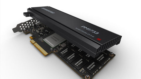
Samsung Brings Revolutionary Software Innovation to PCIe Gen4 SSDs for Maximized Storage Performance
Samsung Electronics Co., Ltd., the world leader in advanced memory technology, today announced that it has brought the latest software innovations to the company’s most cutting-edge PCIe Gen4 solid state drive (SSD) series, opening up a new paradigm in SSD performance.
Nano Bulb Lights Novel Path
What may be viewed as the world’s smallest incandescent lightbulb is shining in a Rice University engineering laboratory with the promise of advances in sensing, photonics and perhaps computing platforms beyond the limitations of silicon. Gururaj Naik of Rice’s Brown School of Engineering and graduate student Chloe Doiron have assembled unconventional “selective thermal emitters” — collections of near-nanoscale materials that absorb heat and emit light.
The Future of ‘Extremely’ Energy-Efficient Circuits
Data centers are processing data and dispensing the results at astonishing rates and such robust systems require a significant amount of energy — so much energy, in fact, that information communication technology is projected to account for 20% of total energy consumption in the United States by 2020. To answer this demand, a team of researchers from Japan and the United States have developed a framework to reduce energy consumption while improving efficiency.
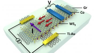
Scientists Create Fully Electronic 2-Dimensional Spin Transistors
Physicists from the University of Groningen constructed a two-dimensional spin transistor, in which spin currents were generated by an electric current through graphene.
SEMICON Taiwan 2019 Opens with Smart Tech, Innovation, Digital Future in Spotlight
With Taiwan expected to lead the world in semiconductor equipment investments in 2019, SEMICON Taiwan 2019 opens today, gathering the world’s top technologists, visionaries and innovators for insights into the latest trends and opportunities across smart vertical markets including manufacturing, automotive, healthcare and data. September 18-20 at Nangang Exhibition Center, Hall I, in Taipei, SEMICON Taiwan 2019 spans the entire semiconductor and microelectronics supply chain – from design through systems.
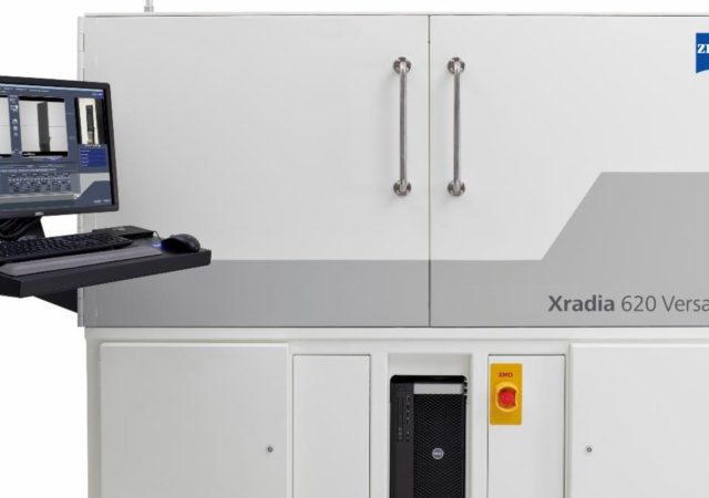
ZEISS Accelerates Time to Market for Advanced Semiconductor Packages with Non-destructive 3D X-ray Measurement Solution
ZEISS today introduced the ZEISS Xradia 620 Versa RepScan — a submicron-resolution, 3D non-destructive imaging solution for inspection and measurement that accelerates time to market for advanced IC packages.
D2S Enables “Stitchless” Full-Chip Inverse Lithography Technology in a Single Day for The Multi-Beam Era
D2S today introduced TrueMask® ILT, a GPU-accelerated hardware and software system that enables IC manufacturers to implement stitchless, full-chip inverse lithography technology (ILT) for advanced-node designs in a single day.
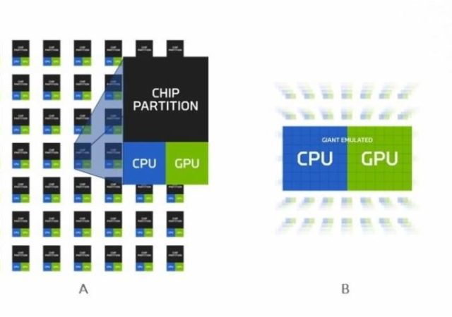
Intel Updates Advanced Packaging Technologies at SEMICON West Part 2
At the Architecture Day Intel demoed a Foveros-based part, comprising a high-performance 10-nm chiplet on a low-power 22nm base die. The upper die contained five cores, four Atom low-power cores and a high-performance core, and as shown in the Intel image above, the two lower dies were stacked with PoP memory, all in a 12 x 12 mm package with 2mW standby power.