
At SEMICON Southeast Asia 2021, Mr. Terence Gan, SVP, Semiconductors, Economic Development Board (EDB) of Singapore, outlined five research pillars.
JEDEC publishes XFM Embedded and Removable Memory Device Standard
JEDEC announced the publication of JESD233: XFM Embedded and Removable Memory Device (XFMD) standard.
onsemi to Acquire GT Advanced Technologies
ON and GT Advanced Technologies, a producer of SiC, entered into a definitive agreement under which onsemi will acquire GTAT for $415 million in cash.
Mitsubishi Chemical Advanced Materials to Become Climate Neutral By 2023
MCAM has set ambitious targets and actions to reduce its emissions and environmental impact, compensate for unavoidable emissions with high-quality carbon credits, and invest in carbon removal projects

New Plating Tool for WLP and Plating in Compound Semi Manufacturing
ACM’s Ultra ECP GIII plating tool is designed for WLP for compound semiconductors, with product offerings for SiC, GaN and GaAs. The tool is also capable of plating gold into backside deep hole processes with greater uniformity and better step coverage.

Intel Wins US Government Project to Develop Leading-Edge Foundry Ecosystem
Intel Foundry Services will lead the first phase of the U.S. Department of Defense’s RAMP-C program to establish a domestic commercial foundry infrastructure.
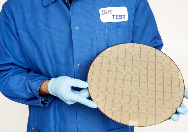
IBM Unveils On-Chip Accelerated Artificial Intelligence Processor
At the annual Hot Chips conference, IBM unveiled details of the upcoming new IBM Telum Processor, designed to bring deep learning inference to enterprise workloads to help address fraud in real-time.
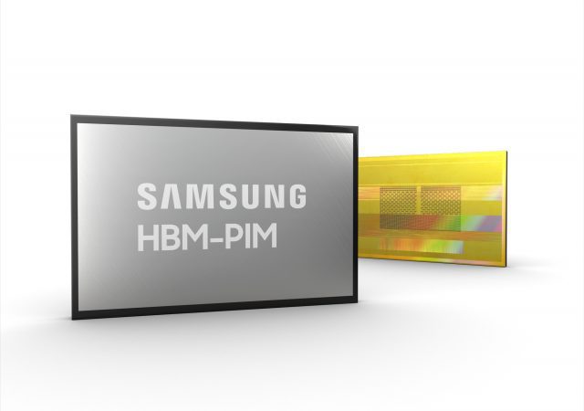
Samsung Brings In-memory Processing Power to Wider Range of Applications
Samsung’s revelations at Hot Chips include the first successful integration of its PIM-enabled High Bandwidth Memory (HBM-PIM) into a commercialized accelerator system, and broadened PIM applications to embrace DRAM modules and mobile memory.
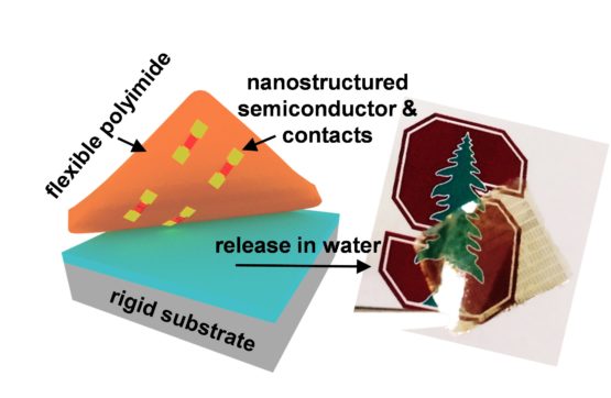
Researchers Just Developed New High-Performance Flexible Electronics
The manufacturing technique invented by the Stanford team makes it possible to create flexible and atomically thin transistors that are several times smaller than previous efforts.
Wooptix Introduces Wafer Geometry System for 300mm Blank Silicon Wafers
Wooptix SL, a Spanish company dedicated to developing new imaging solutions, has introduced Phemet® lab system, a 300mm blank silicon wafer geometry system collecting millions of topography data points on a full wafer in a few seconds.