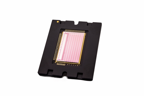
Silicon chip technology has surprising and largely untapped possibilities for product innovation. But reliably fabricating these specialty chips requires a multidisciplinary team and a robust plan.
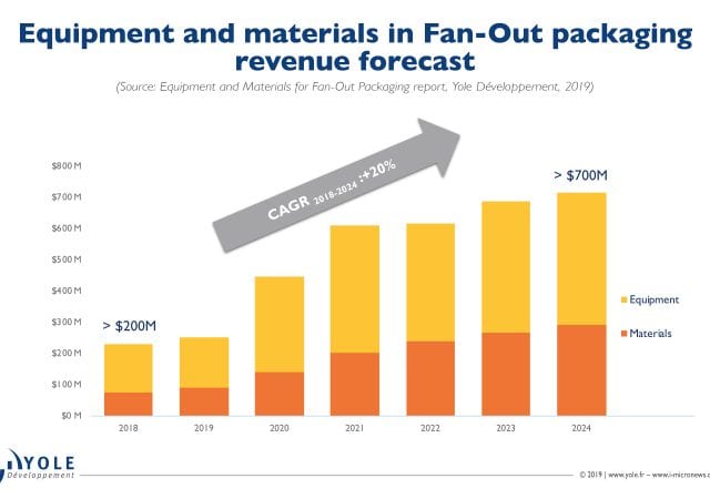
A New Wave of Fan-Out Packaging Growth
Key players from different business models are fueling new growth.
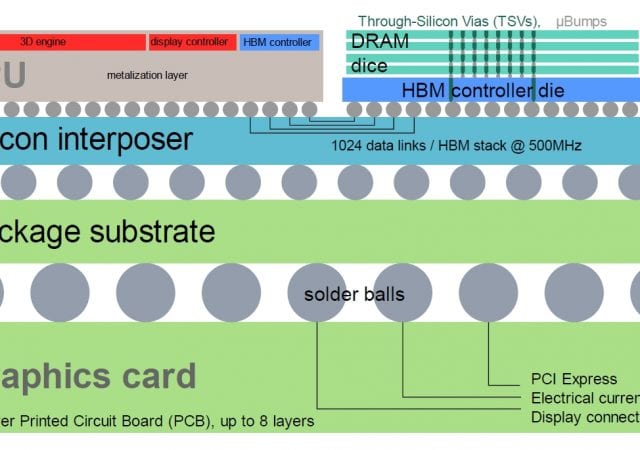
The History and Future of DRAM Architecture in Different Application Domains: An Analysis
Common trends and bottlenecks in DRAM architecture are identified.
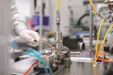
Swagelok Introduces New ALD20 UHP Valve
The ALD20’s patent-pending design maximizes production process efficiency and deposition consistency by providing flow coefficients two to three times what can be achieved using today’s standard ALD valve technology.
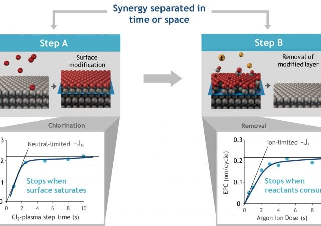
Nanoscale Features through Atomic Layer Processing
Atomic layer etching and deposition processes offer atomic scale control through the use of self-limiting reactions.
SLO Cables for Vacuum Application
A new solution that combines ‘super’ low outgassing (SLO) cables with flexibility and integration of multiple cables is designed for applications with moving parts in vacuum chamber environments ranging from motors to encoders.
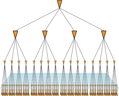
Clock Tree Optimization Methodologies for Power and Latency Reduction
Widely used clock structures are described, with an emphasis on practical implementations of conventional clock tree structures along with H-Tree.
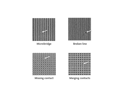
EUV Lithography: Sailing Along the Stochastic Cliffs
Stochastic printing failures are random, non-repeating, isolated defects such as microbridges, locally broken lines and missing or merging contacts.
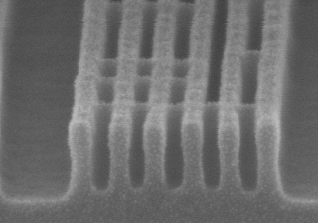
EUV Lithography: Weighing the Options for Future Logic and Memory Applications
Imec takes a great leap forward in understanding and pushing the limits of extreme ultraviolet lithography – part I
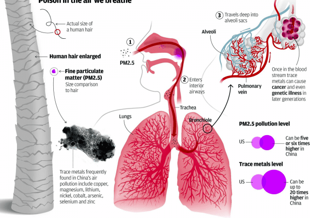
Abating Potentially Dangerous Particles 2.5 µm and Smaller
Particles, especially fine particles, are very important because of their impact on human health.