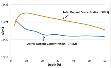
Electrical property depth profile data from semiconductor films can be obtained using the Differential Hall Effect Metrology approach. The technique can yield sub-nm depth resolution for Si and Ge. For III-V compounds depth resolution is ~1 nm.
The Holistic Approach to Materials and Processing for New and Scaled Devices
Taking a holistic approach to materials integration considering the subtle effects of seemingly simple materials challenges is required to ensure performance, yield, reliability, and overall cost of ownership.
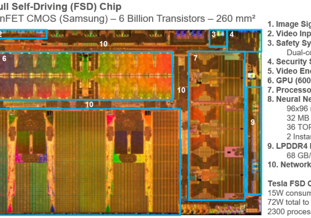
A Deep Dive into AI Chip Arithmetic Engines
Tesla’s autopilot chip executes 72-trillion additions and multiplications per second: It better get the math right
Revolutionizing Wafer Testing to Bring New Technologies to Market
Nearly every new technology breakthrough in the semiconductor industry targets high volume manufacturing and comes with its unique specificities. This results in challenges for engineers to manufacture and test new integrated circuits (ICs) on the wafer.
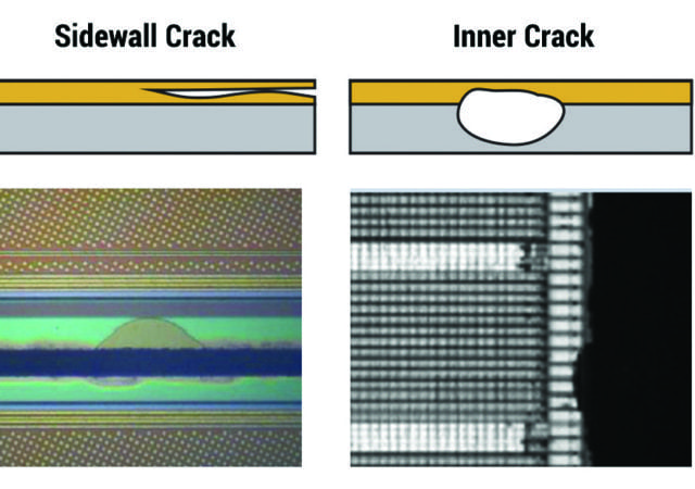
Die Crack Detection in HVM is Critical for High Reliability Applications
The detection of cracks after the wafer is diced into individual die has become critical in high reliability applications, like the automotive market, where there are substantial safety and liability concerns.
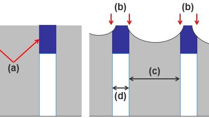
Building Stronger, Better Designs with DTCO CMP Modeling and Simulation
Predicting CMP damage has always been a part of the manufacturing process, but in a Design-technology co-optimization (DTCO) flow, foundries and EDA companies can work together to automate CMP model building and simulation.
Innovative Approaches to Vacuum Enable High-Volume Atomic Layer Processing
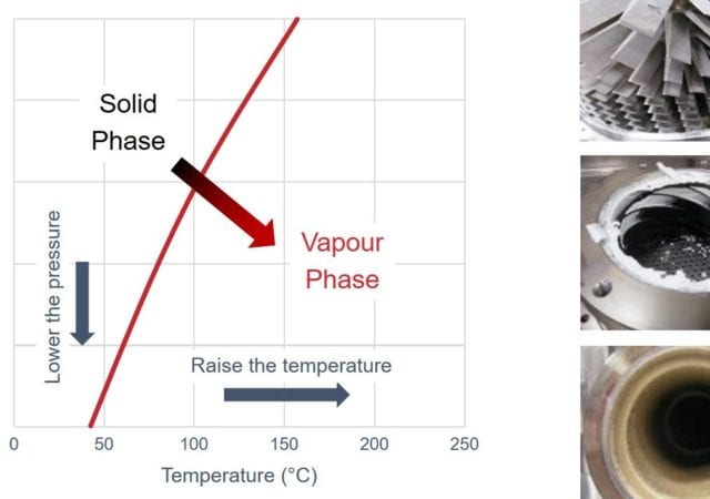
Processes such as atomic layer deposition and etch require fast, repetitive, complete exchange of gases in the process chamber. Vacuum equipment manufacturers have responded with solutions that address the challenges presented by these high flow applications.
Process Watch: A Statistical Approach to Improving Chip Reliability
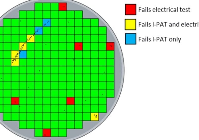
The Process Watch series explores key concepts about process control—defect inspection, metrology and data analytics—for the semiconductor industry. This article is the fifth in a series on process control strategies for automotive semiconductor devices.
Examining Chip Manufacturing Challenges for Advanced Logic Architecture
A look at the critical issues that will have to be addressed to cost-effectively produce the next generation of faster, denser chips.
Process Control Needs Are Increasing Across Semiconductor Fabs
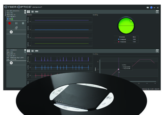
To increase yields and tool uptime, there is a growing need in the front-end of the fab to use wireless sensors.
