GILAD REUT, Product Marketing Manager, Process Diagnostics and Control, Applied Materials
Optical Patterned Wafer Inspection (OPWI) faces challenges as semiconductor designs become increasingly complex in the era of EUV lithography, multi-patterning and 3D transistor architectures. In advanced manufacturing nodes, the physical dimensions of critical defects are well below the optical resolution of OPWI systems. Consequently, differentiating between yield-killing and nuisance defects becomes extremely challenging, resulting in high false alarm rates and requiring larger budgets (i.e. more images) for eBeam review.
To address this ever-increasing challenge, novel Deep Learning (DL) and Artificial Intelligence (AI) detection and filtering algorithms are necessary to improve the separation between Defects of Interest (DOI) and false defects. In this article, we present innovative DL and AI algorithms that are employed by an advanced Brightfield optical inspection system to enhance the detection of yield-killing defects and improve the filtering of nuisance defects for 2nm technology nodes and beyond.
Optical inspection
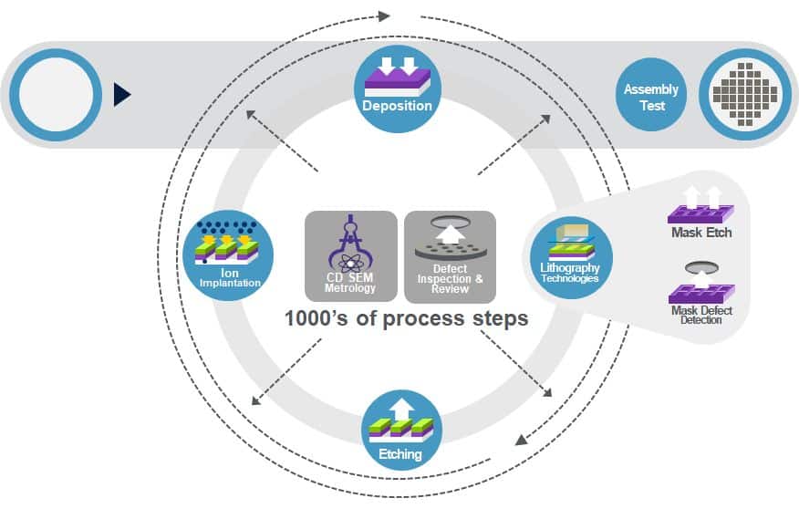
Wafer defects have a well-known impact on device yield, and timely identification of their root cause is crucial for high fabrication yield and accelerated process development (FIGURE 1). Early detection and fast correction can have a critical impact on fab operations, saving chipmakers millions of dollars a day. There are two complementary systems for detecting defects: inspection and review. Optical inspection systems are used to identify potential defects on the wafer. Subsequently, Scanning Electron Microscope (SEM) review systems provide the higher resolution necessary for classifying and characterizing different defect types.
The specific architecture of an optical inspection system depends on its target application space, but they all share some basic principles and modules: light source, illumination path, objective, XY stage, collection path, detectors and image processing (FIGURE 2).
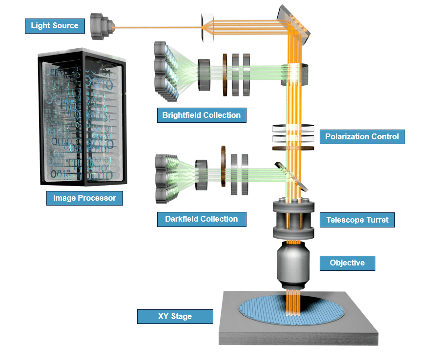
During the inspection process, the wafer is scanned with a light beam. Reflected (Brightfield) and scattered (Darkfield) light are collected using dedicated collection paths and detectors, and a pixel-level signal is transmitted to the image processor to generate large numbers of in-die images. The wavelength of the light source and the numerical aperture of the objective determines the resolution of the images. A typical full-wafer scan produces many trillions of pixels.
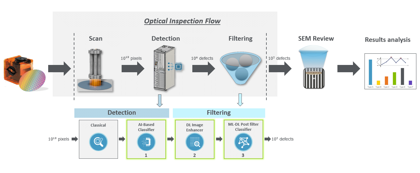
The subsequent defect detection process can be described as a funnel with several steps. In each step, the number of suspected defects is reduced until we end with a final defect map that typically contains several hundreds of suspected defects.
In the first funnel, the collected images are compared to one another to detect suspected defects. As part of the detection algorithm, an image with a suspected defect (referred to as the Current image) is compared to other images from a similar region on the wafer or die (known as Reference images, assumed to be non-defective) to create a Difference image. The Difference image shows the difference between the Current and Reference images. If the pixels in the Current and Reference images are similar, indicating no defect, the resulting Difference pixels will be dark. On the other hand, if the Current and Reference pixels are different, indicating a defect, the resulting pixels will be bright. Consequently, in the case of a true defect, the Difference image will typically be dark with a bright spot or vice versa. For all suspected defect images, the Signal-to-Noise Ratio (SNR) is calculated. If the SNR of a pixel (or group of pixels) exceeds a predefined threshold, that pixel will be marked as a suspected defect.
In the second phase, a filtering algorithm is employed to distinguish between yield-killing defects and nuisance defects using various attributes associated with the suspected defects. This process reduces the quantity of suspected defects from millions to thousands or even hundreds.
The extremely small feature sizes of leading-edge transistors make yield-killing defects difficult to differentiate from noise, and small variances evolve into yield-killing defects that are well below the resolution of the optical inspection systems. This problem grows as semiconductor designs become increasingly complex and involve EUV lithography, multi-patterning steps and the fabrication of 3D structures such as Gate All Around (GAA) transistors. To confront this ever-increasing challenge of nuisance suppression, novel DL and AI detection and filtering algorithms are adopted to enhance the performance of the detection flow (FIGURE 3).

The authors present three innovative DL and AI algorithms that are employed by an advanced Brightfield optical inspection system to enhance the detection of yield-killing defects and improve the filtering of nuisance defects for cutting-edge 2nm technology nodes. Read the full article in Semiconductor Digest magazine.