Today’s semiconductor manufacturing facilities are marvels of the modern world. Construction requires billions of dollars in capital expenditures (CapEx) and millions of workhours within a short period of time. And a lot of them are scheduled to come on-line in the coming years.
The semiconductor industry is expected to start 18 new fab construction projects in 2025, according to SEMI’s latest quarterly World Fab Forecast report. The new projects include three 200mm and fifteen 300mm facilities, the majority of which are expected to begin operations from 2026 to 2027. Longer term, the industry plans to begin operation of 97 new high-volume fabs. This includes 48 projects in 2024 and 32 projects set to launch in 2025, with wafer sizes ranging from 300mm to 50mm.
Many new fabs are huge: According to Herbert Blaschitz, executive VP, global business unit advanced technology facilities (ATF), Exyte – who spoke at the recent SEMI Industry Strategy Symposium (ISS) – fabs require >$20 billion overall CapEx investment, with $4-6 billion of that just for the facility. Exyte has been involved with the construction of close to 300 fabs in its 30 year history. Construction requires 30-40 million workhours to manage 83,000 tons of steel reinforcement, 5,600 miles of cabling and 785,000 cubic yards of concrete.
Such fabs can consist of a 430,000 ft2 (40,000 m2) cleanroom, housing 2000 process tools, with an average of 50 individual process and utilities connections per tool. That’s over 50,000 process & utilities connections!
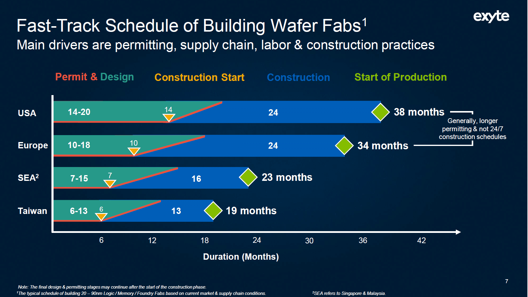
One of the challenges facing fab builders in the U.S. and Europe is how efficient Taiwan has become (closely followed by China and Southeast Asia). As an example, Blaschitz showed a very large fab facility that had been built in Taiwan in about 20 months (he declined to name the company but said it was U.S.-owned). By comparison, he said fabs in the U.S. take 38 months to build, from permitting and design to the time when they can start wafer production. It’s 34 months for fabs in Europe.

Similarly, construction costs in the U.S., compared to Taiwan, are about twice as much (the process equipment costs are similar). “Building a wafer fab in the west costs twice as much and takes twice the time of building it in Taiwan,” Blaschitz said.
One of the main reasons? Experience: “Their supply chain is just unbelievably good. And very often it’s not that they are much more precise, but they know what they are doing,” Blaschitz said. “If you look at a drawing in Taiwan, half of the things what you have in the western world are missing. They don’t need those detailed information; they do it every day and that makes them very productive.”
The CHIPS Act in the U.S. is designed to help overcome this imbalance, but it’s not enough. Blaschitz said the best solution is to use what he calls “virtual commissioning,” which begins during the planning and the design phase. “With the digital twin, we can basically commission the fab without the fab being built,” he said. This helps to spot obstacles and even reduce operating costs and carbon emissions. Semiconductors being used to better build more semiconductors – gotta love it!