Silicon Valley Hall of Famer and Founder of Lam Research to present unsurpassed levels of on-chip security enabled by Multicolumn E-beam Lithography (MEBL)
Design
SEMI Talent Forum to Help Build Next-Generation Chip Industry Workforce
Post-graduates and onboarding talent will connect with local companies to explore semiconductor industry career paths and employment opportunities at the SEMI Talent Forum, 6 March 2020 in Swansea, UKat the University of Swansea. Sponsored by SEMI, the industry association representing the global electronics manufacturing and design supply chain, and staged in partnership with European organizations including the University of Swansea, Edwards, Oxford Instruments, and SPTS Technologies, the event will also highlight how technology is reshaping the global workforce. Participation is free of charge and registration is open.
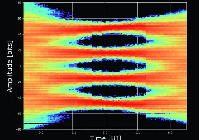
SerDes Designs: Keeping Pace with a Demanding Network Environment
As speed, signal integrity and test boundaries are pushed, cycles of architectural changes and new levels of design innovation for the SerDes chip are only a few of the challenges.
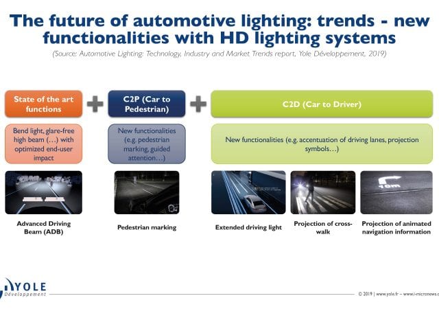
Pixel LED Headlights: High Definition Technology Enables New Driving Experiences
LEDS serve as the key technology for the attractive styling of headlights and definition of brand signatures.
Onto Innovation Announces Multiple Orders to Support 5G Ramp
Onto Innovation Inc. (NYSE: ONTO) announced that it has received orders totaling 15 systems from two leaders in advanced packaging. Both customers are ramping up to support the ongoing demand for 5G smartphones which drives advanced packages requiring more precise process control solutions.
Designing and Fabricating Fully-Customized Chips
Silicon chip technology has surprising and largely untapped possibilities for product innovation. But reliably fabricating these specialty chips requires a multidisciplinary team and a robust plan.
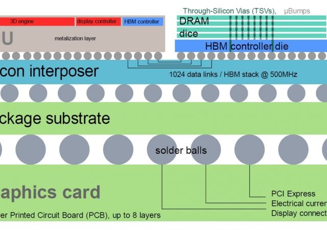
The History and Future of DRAM Architecture in Different Application Domains: An Analysis
Common trends and bottlenecks in DRAM architecture are identified.
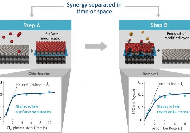
Nanoscale Features through Atomic Layer Processing
Atomic layer etching and deposition processes offer atomic scale control through the use of self-limiting reactions.
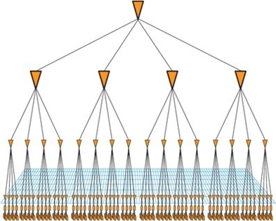
Clock Tree Optimization Methodologies for Power and Latency Reduction
Widely used clock structures are described, with an emphasis on practical implementations of conventional clock tree structures along with H-Tree.
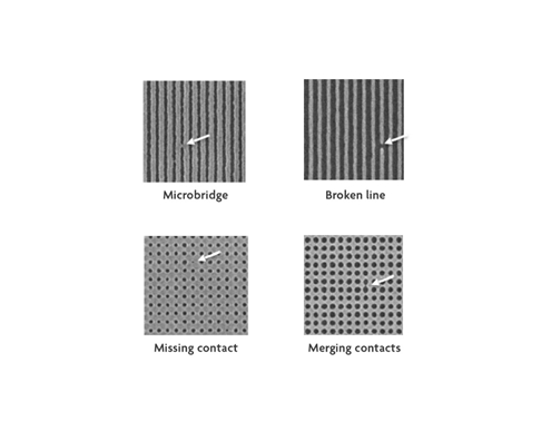
EUV Lithography: Sailing Along the Stochastic Cliffs
Stochastic printing failures are random, non-repeating, isolated defects such as microbridges, locally broken lines and missing or merging contacts.