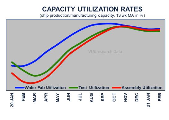
The shortage of semiconductors won’t be easy to solve, with some equipment lead times stretching out several years, said VLSI Research CEO Dan Hutcheson at a SEMI event.
Editor’s Picks

Semiconductor Materials Supply-Chain Shortages
TECHCET CA LLC’s prediction of a wet chemical supply fallout is materializing.

What’s in the March Issue?
Each issue of Semiconductor Digest has articles found only in the magazine! Read the March issue…

Intel Launches ‘IDM 2.0’ Strategy, Including Two New U.S. Fabs and Foundry Services
Intel’s new CEO Pat Gelsinger announced significant manufacturing expansion plans, starting with an estimated $20 billion investment to build two new factories fabs in Arizona. He also announced Intel’s plans to become a major provider of foundry capacity in the U.S. and Europe to serve customers globally.
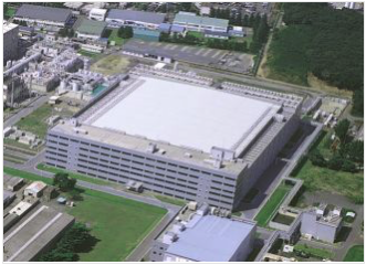
Fire Destroys Part of Renesas Fab, Fueling Supply Concerns
Part of the processes in the N3 Building of the Naka Factory caught fire on March 19, an event which has halted production on the 300mm line for likely the next month.
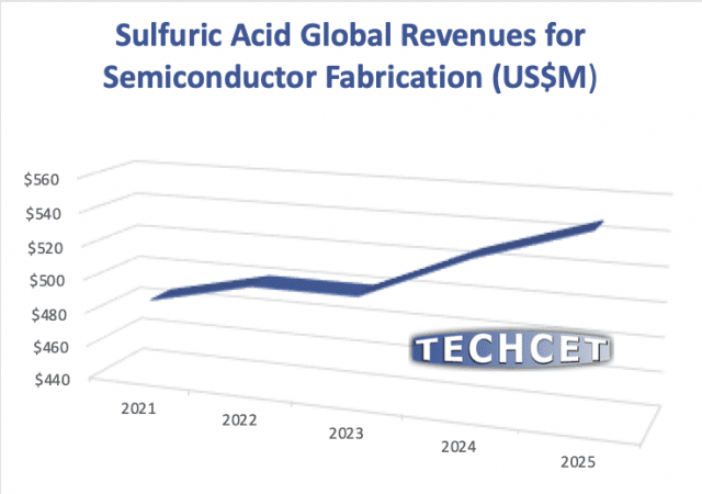
Investment Needed in US$500M Sulfuric Market
IC fabs “life blood” may soon be in short supply in US.
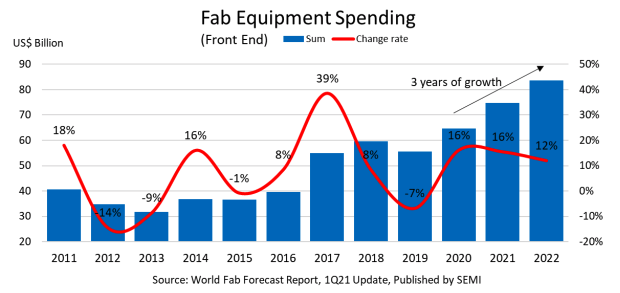
Global Fab Equipment Spending Poised to Log Three Straight Years of Record Highs
Fueled by surging pandemic-inspired demand for electronics devices, the global semiconductor industry is on track to register a rare three consecutive years of record highs in fab equipment spending with a 16% increase in 2020 followed by forecast gains of 15.5% this year and 12% in 2022.
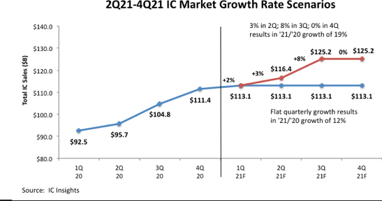
IC Insights Raises Its 2021 IC Market Forecast from 12% to 19% Growth
Rising market expectations are being witnessed across most IC product lines from Analog to Logic to DRAM.
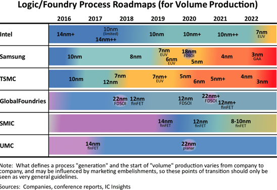
Revenue per Wafer Climbs as Demand Surges for 5nm/7nm IC Processes
Despite high development costs, smaller nodes bring greater revenue per wafer.
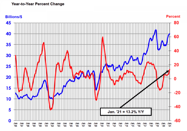
Global Semiconductor Sales Increase 13.2% Year-to-Year in January
Month-to-month sales tick up 1.0% worldwide during first month of 2021.
