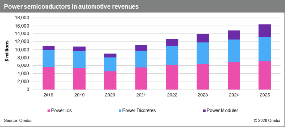
The COVID-19 pandemic is wreaking havoc on sales of automotive power semiconductors, with falling demand for motor vehicles causing global market revenue to decline by 16 percent in 2020.
Editor’s Picks
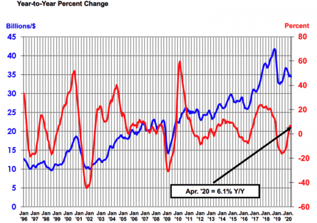
Global Semiconductor Sales Decrease 1.2 Percent Month-to-Month in April
Sales in April increase 6.1 percent year-to-year; disruptions from the COVID-19 pandemic have so far not substantially impacted overall global sales
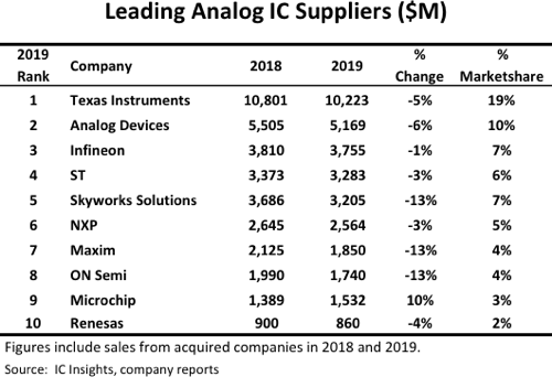
Texas Instruments Maintains Firm Grip As World’s Top Analog IC Supplier
TI’s 2019 analog marketshare grew to 19% and ST climbed to fourth place as the top-10 suppliers collectively accounted for 62% of total analog sales.

Why Restarting the Global Economy Won’t be Easy
As the world contemplates ending a massive lockdown implemented in response to COVID-19, Vinod Singhal is considering what will happen when we hit the play button and the engines that drive industry and trade squeal back to life again.
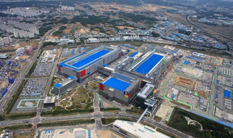
Samsung Electronics Expands its Foundry Capacity with A New Production Line in Pyeongtaek, Korea
Samsung today announced plans to boost its foundry capacity at the company’s new production line in Pyeongtaek, Korea, to meet growing global demand for cutting-edge extreme ultraviolet (EUV) solutions.

Telehealth to Experience Massive Growth with COVID-19 Pandemic, Says Frost & Sullivan
Frost & Sullivan’s recent analysis, Telehealth—A Technology-Based Weapon in the War Against the Coronavirus, 2020, finds that the demand for telehealth technology is expected to rise dramatically as the COVID-19 pandemic continues to disrupt the practice of medicine and the delivery of healthcare worldwide.
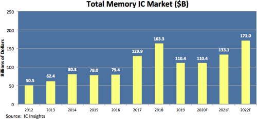
Memory Market Not Forecast to Exceed 2018 High of $163.3B until 2022
The most current 2017-2024 forecast for 35 major IC product segments (e.g., DRAM, 16-bit MCUs, power management analog devices, etc.) by market, unit shipments, and ASP was presented in the April Update to the 2020 edition of The McClean Report—A Complete Analysis and Forecast of the Integrated Circuit Industry (MR20).
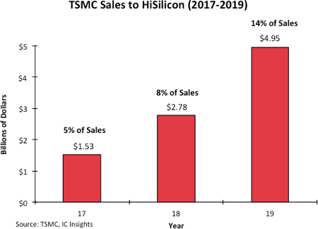
HiSilicon First China-Based Semi Supplier to be Ranked in Top-10
Top-10 semiconductor suppliers log strong 16% jump in 1Q20/1Q19 sales.
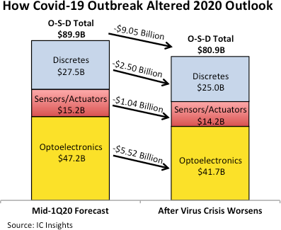
Virus Crisis Hits Optoelectronics, Sensors/Actuators, and Discretes
After 10 years of record-high sales, combined revenues for optoelectronics, sensors/actuators, and discrete semiconductors are expected to drop 6% in virus-plagued 2020, says the new O-S-D Report.
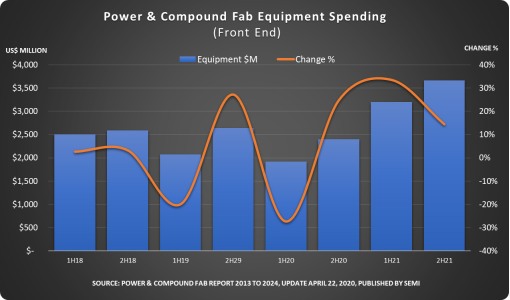
Power and Compound Fab Spending to Rebound in Second Half of 2020, Set New Record in 2021
The 2020 rally will help blunt a drop in annual spending, now projected at 8 percent, as fabs ride the COVID-19 recovery wave.