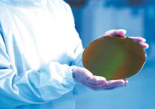
The Semiconductor Industry Association (SIA), in collaboration with the Semiconductor Research Corporation (SRC), today announced the winners of its 2019 University Research Awards.
Ed’s Threads
Ruthenium Nanolayers are Ferromagnetic at RT
Researchers from Intel Corporation and the University of Minnesota and the University of Wisconsin have shown that strained atom-scale films of pure ruthenium (Ru) metal exhibit ferromagnetism at room temperature, openning up the possibility of using the material to build novel magnetic random access memory (MRAM) devices. As per details recently published in Nature Communications (https://doi.org/10.1038/s41467-018-04512-1), Ru thin films with a thickness of 2.5, 6, or 12 nm, were grown on…
Mott Memristor Chaos could make Efficient AI
Congratulations to Suhas Kumar, John Paul Strachan, and R. Stanley Williams of Hewlett Packard Labs in Palo Alto for showing not just how to make a Mott memristor, but that you can create controlled chaos with one. “We showed that this type of memristor can generate chaotic and nonchaotic signals,” says Williams, who invented the memristor based on theory by Leon Chua. An analysis of the material science and engineering…
MEMS Mirrors for LIDAR
Clever integration of new microelectronic/nanoelectronic technologies will continue to provide increased functionalities for modern products. Light Imaging, Detection, And Ranging (LIDAR) technology uses lasers to see though fog and darkness, and smaller less expensive LIDAR systems are needed for autonomous driving applications now being developed by dozens of major companies around the world. A significant step in the right direction has been taken by the US government’s Lawrence Livermore National…
Moore’s Law Smells Funny
…maybe we need “Integrated Cleverness Law” “Jazz is not dead, it just smells funny.” – Frank Zappa 1973 from Be-Bop Tango (Of The Old Jazzmen’s Church) Marketing is about managing expectations. IC marketing must position next-generation chips as adding significant new/improved functionalities, and for over 50 years the IC fab industry has leaned on the conceptual crutch of “so-called Moore’s Law” (as Gordon Moore always refers to it) to do…
Flagello to receive Zernike Award at SPIE Advanced Lithography
Donis Flagello, president, CEO, and COO of Nikon Research Corporation of America (NRCA), will be presented with the 2017 Frits Zernike Award for Microlithography on Monday 27 February during SPIE Advanced Lithography in San Jose, California. The award, presented annually for outstanding accomplishments in microlithography technology, recognizes Flagello’s leading role in understanding and improving image formation in optical lithography for semiconductor manufacturing. A prominent member of the industry since the…
Photoelectric measure of atomically thin stacks
A team led by researchers at the University of Warwick have discovered a breakthrough in how to measure the electronic structures of stacked 2D semiconductors using the photoelectric (PE) effect. Materials scientists around the world have been investigating various heterostructures to create different 2D materials, and stacking different combinations of 2D materials creates new materials with new properties. The new PE method measures the electronic properties of each layer in…
XMC becomes YRST or Changjiang Storage
As reported by Digitimes, a major enterprise in Wuhan, China has broken ground on the first of three mega-fabs to produce 3D-NAND chips. The final fab name-plate may ultimately read XMC or YMTC or YRST or possibly Changjiang Storage (not to be confused with GuangDong ChangJiang Storage Battery), but it is over half owned by the Chinese government’s Tsinghua Unigroup. Total investment in XMC/YRST by Tsinghua Unigroup is reported by…


