A POSTECH research team has recently demonstrated a ferroelectric memory that exceedingly surpasses the performance of the conventional flash memory in terms of operation speed, power consumption, and device reliability.
MEMS
CEA-Leti Reports Machine-Learning Breakthrough that Opens Way to Edge Learning
CEA-Leti scientists have demonstrated a machine-learning technique exploiting what have been previously considered as “non-ideal” traits of resistive-RAM (RRAM) devices, overcoming barriers to developing RRAM-based edge-learning systems.
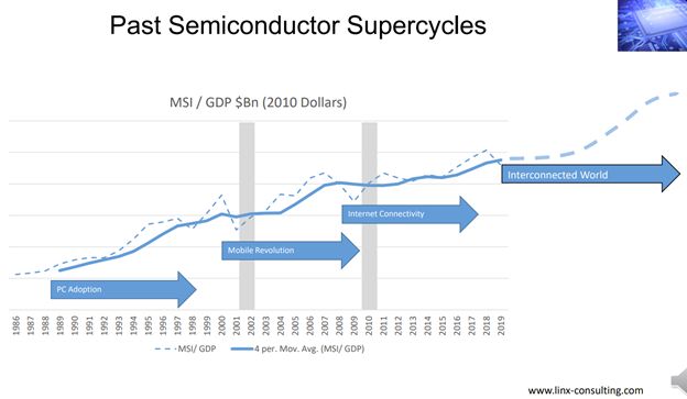
Trillion Dollar Chip Industry Seen at SEMI ISS
The semiconductor industry is entering a “supercycle” as 5G, IoT, AI data analysis converge.
Newly Developed GaN Based MEMS Resonator Operates Stably Even at High Temperature
Liwen Sang, independent scientist at International Center for Materials Nanoarchitectonics, National Institute for Materials Science (also JST PRESTO researcher) developed a MEMS resonator that stably operates even under high temperatures by regulating the strain caused by the heat from gallium nitride (GaN).
Intel Appoints Tech Industry Leader Pat Gelsinger as New CEO
Intel today announced that its board of directors has appointed 40-year technology industry leader Pat Gelsinger as its new chief executive officer, effective Feb. 15, 2021. Gelsinger will also join the Intel board of directors upon assuming the role. He will succeed Bob Swan, who will remain CEO until Feb. 15.
SOI Industry Consortium Joins SEMI as Strategic Association Partner
SEMI today announced that the SOI Industry Consortium, a leading industry organization representing the complete SOI-based microelectronics value chain, has joined SEMI as a Strategic Association Partner effective January 1, 2021.
SEMICON Korea 2021 Goes Virtual With Focus on AI, Sensors, Smart Manufacturing and Talent
Cutting-edge innovations in artificial intelligence (AI), smart manufacturing, sustainable manufacturing, and sensors for a hyper-connected world will take the spotlight at SEMICON Korea 2021 as the event goes virtual February 3-12 to help curb the spread of COVID-19. Registration is open.
ESD Alliance Reports Strong Electronic Design Automation Industry Revenue Growth for Q3 2020
Electronic Design Automation (EDA) industry revenue increased 15% in Q3 2020 to $2,953.9 million, compared to $2,567.7 million in Q3 2019, with all categories logging significant gains, the Electronic System Design (ESD) Alliance Market Statistics Service (MSS) announced today.
PC Sales Remain on Fire as Fourth Quarter Shipments Grow 26.1% Over the Previous Year, According to IDC
With the pandemic still in full swing, traditional PCs (inclusive of desktops, notebooks, and workstations) were once again an in-demand consumer technology.
STMicroelectronics Appointed Rajita D’Souza as President, Human Resources and Corporate Social Responsibility
STMicroelectronics (NYSE: STM), a global semiconductor leader serving customers across the spectrum of electronics applications, announced today the appointment of Rajita D’Souza as President, Human Resources and Corporate Social Responsibility (CHRO). Effective Jan 1, 2021, she reports directly to Jean-Marc Chery, President and CEO and is a member of ST’s Executive Committee.