Hprobe, a provider of semiconductor Automatic Test Equipment (ATE) for magnetic devices, today announced the completion of a new funding round driven by international investors, providing an exceptional depth of expertise, a global ecosystem of partnerships and the endorsement of industry market leaders. The company has raised more than 2 million euros to support its strong international development in the field of spintronics based devices testing, such as MRAMs (Magnetic Random Access Memories) and TMR (Tunnel Magneto Resistance) sensors.
MEMS
Dow Introduces First Solventless Silicone Conformal Coating with UV and Moisture Dual Cure
Dow (NYSE: Dow), introduced today at IPC APEX EXPO 2020 new DOWSIL™ CC-8030 UV and Moisture Dual Cure Conformal Coating, the industry’s first solventless silicone conformal coating with an ultraviolet (UV) and moisture dual cure system for high throughputs. This new environmentally responsible silicone technology promotes sustainability, health and safety while reducing processing costs through automated spraying and fast, energy-efficient UV curing.
2019 Global Silicon Shipments Dip From 2018 Record High But Revenue Remained Stable Above $11 Billion
Worldwide silicon wafer area shipments in 2019 declined 7 percent from the 2018 record high while revenue remained above the $11 billion mark despite a global silicon revenue slip of 2 percent over the same period, the SEMI Silicon Manufacturers Group (SMG) reported in its year-end analysis of the silicon wafer industry. Silicon wafer area shipments in 2019 totaled 11,810 million square inches (MSI), while the industry logged shipments of 12,732 million square inches in 2018. Revenues in 2019 totaled $11.15 billion, edging down from the $11.38 billion posted in 2018.
CEA-Leti Develops Tiny Photoacoustic-Spectroscopy System For Detecting Chemicals & Gases
Leti, an institute of CEA-Tech, has developed a photoacoustic spectroscopy technology for monitoring dangerous chemical emissions and traces of gas that could reduce the cost and the size these systems by a factor of 10 or more compared to existing tools. To be presented in an invited paper at Photonics West 2020 titled “Micro PA detector: pushing the limits of mid-IR photoacoustic spectroscopy integrated on silicon”, the detector also provides high immunity to external noise and high sensitivity and selectivity.
SEMI Postpones SEMICON China, Suspends SEMICON Korea in Response to Coronavirus Outbreak
In accordance with government guidelines and to protect the health and safety of exhibitors and guests, SEMI announced Tuesday the postponement of SEMICON/FPD China 2020 and related events originally scheduled for March 18-20, 2020. SEMI China is actively working on a contingency plan for rescheduling of the event and will keep you informed as soon as a confirmed plan is in place.

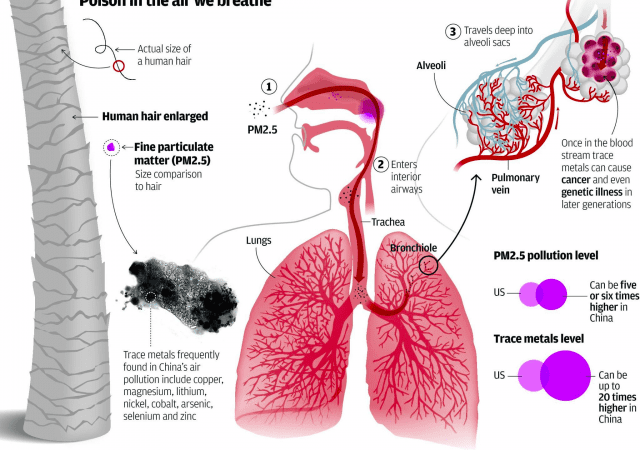
Abating Potentially Dangerous Particles 2.5 µm and Smaller
Particles, especially fine particles, are very important because of their impact on human health.
CEA-Leti Clears a Path to Developing Ultralow Loss, High-Power Photonics in UV through Mid-Infrared Wavelengths
Leti, an institute of CEA-Tech, has developed a silicon nitride (Si3N4) 200mm platform for developing ultralow loss, high-power photonics in UV through mid-infrared wavelengths. Available in CEA-Leti’s SiN platform in a multi-project-wafer program, the breakthrough targets designers in integrated quantum optics, LiDAR, biosensing, and imaging whose projects require ultralow propagation losses and high-power handling capability.
BJG Electronics Group Names Kent Smith as President
New York based BJG Electronics Group announced today that Kent Smith has joined the company as President, effective February 3, 2020. Most recently serving as Chief Commercial Officer for Integrated Supply Network, Smith brings to BJG a track record of successful leadership positions at electronics industry leaders. At Nu Horizons Electronics Corp., he served as President of the Americas and Asia-Pacific. Later, as Vice President of Sales at Arrow Electronics, he led a team that generated more than $4 billion in annual sales.
Coronavirus Outbreak Can Drastically Impact the Technology Road Map for 2020, says GlobalData
The coronavirus outbreak is now entering a crucial phase with the WHO declaring it as a global health emergency. While the economic impact of the outbreak will be dependent on how long it ultimately lasts, its impact on technology markets across the world is already beginning to come to the fore, says GlobalData, a leading data and analytics company. Several technology companies, including Amazon, Microsoft and Apple have now imposed travel restrictions to and from China, whereas Google has altogether suspended its office operations in mainland China, Hong Kong and Taiwan.
CyberOptics Introduces New In-Line Particle Sensor as an Extension of the Industry-Leading Particle Sensing Technology at SPIE
CyberOptics Corporation (NASDAQ: CYBE), a global developer and manufacturer of high-precision 3D sensing technology solutions, will exhibit at SPIE Advanced Lithography from February 25-26, 2020 at the San Jose Convention Center in California, booth #308. During the show, the company will introduce its new In-Line Particle Sensor (IPS) with CyberSpectrum software for semiconductor tool set-up and equipment diagnostics.