Lam Research Corp. today announced that Ava Harter has joined its executive leadership team as senior vice president and chief legal officer.
MEMS

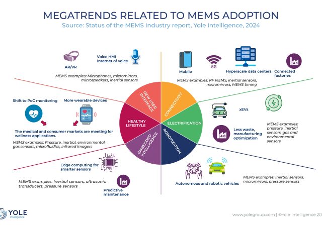
MEMS Industry: Poised for a Resilient Comeback?
Despite challenges, the MEMS industry is set for robust growth and technological advancements.
Advanced Energy Unveiled New Smart Monitoring and Digital Control Capabilities for AC-DC High Power Supplies
Advanced Energy has unveiled a new hardware accessory for its ultra-efficient, high-power suppliers. AE’s PowerPro Dongle unlocks real-time powerful monitoring, control and diagnostics capabilities for designers.

Inorganic Ventures acquires PURE Analytical Laboratories
IV Labs Inc, the parent company of Inorganic Ventures, has acquired PURE Analytical Laboratories in a move to produce materials with higher purities than currently available and to create new, high-purity materials for emerging applications from semiconductors and computing to pharmaceuticals and diagnostic equipment.
Intel Launches Its First US Apprenticeship for Manufacturing Facility Technicians
The program will train facility technician apprentices over the next five years in Arizona.

EV Group’s EVG880 LayerRelease System Wins 2024 Best of West Award
The EVG®880 LayerRelease system from EV Group (EVG) has won the 2024 Best of West award, SEMI and Semiconductor Digest announced today at SEMICON West 2024 at the Moscone Center in San Francisco.
Kaman Measuring Highlights High Precision Displacement Sensors for Extreme Environments
The Measuring Division of Kaman Precision Products, Inc. highlights the availability of high precision displacement sensors for extreme environments such as power generation including nuclear and aerospace propulsion, materials research and development, with operating temperatures from -320°F to +1000°F (+1200°F short term) at pressures up to 5000 psi.
SEMI Americas Announces New Annual Event, SEMIEXPO In The Heartland, Focused on Smart Manufacturing and Smart Mobility
Event partners include the Indiana Economic Development Corporation, the Applied Research Institute, Purdue University, and Visit Indy.
Park Systems Introduces Park FX200, Advanced AFM for 200mm Samples
Park Systems, a manufacturer of nano-metrology systems, announces the release of its latest atomic force microscopy (AFM) innovation, Park FX200, designed for 200mm samples.

Detecting Defects in Tomorrow’s Technology
New research enhances our understanding of a likely candidate for next-generation computer chips.