Singular Photonics emerged from stealth mode today, launching a new generation of image sensors based on single photon avalanche diodes (SPADs).
Packaging
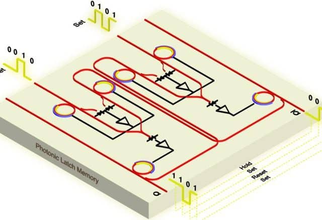
New Optical Memory Unit Poised to Improve Processing Speed and Efficiency
Fast, versatile volatile photonic memory could enhance AI, sensing and other computationally intense applications.
MACOM Signs Preliminary Memorandum of Terms for Federal CHIPS and Science Act Funding
Today, the Healey-Driscoll administration celebrated MACOM Technology Solutions Inc. (MACOM), the Lowell-based manufacturer that develops and supplies semiconductor components to the commercial and defense sectors, signing a preliminary memorandum of terms with the federal government for funding under the CHIPS for America program.
Boosting AI Model Size and Training Speed with Lightwave-Connected Chips
AI growth is capped by data transfer rates between computing chips, but transferring data with light could remove the ceiling.
ASU Selected as Home and Partner for CHIPS and Science Act-Funded National Lab for Semiconductor Advanced Packaging
Following a week where a spirited effort by the Sun Devil football team captured the nation’s attention in the Peach Bowl, it is Arizona State University’s capability as a top-tier research university that has delivered ASU a momentous national win to kick off 2025.
IEEE Electronic Components and Technology Conference Announces Best & Outstanding Papers from ECTC 2024
The IEEE Electronic Components and Technology Conference (ECTC), the world’s premier technical conference and product exhibition for the semiconductor packaging industry, has announced the winners of its prestigious Best and Outstanding Paper Awards for 2024.
Advanced Semiconductor Packaging Market to Generate US$ 40.3 Billion in Revenue by 2031
The Advanced Semiconductor Packaging Market, valued at US$ 30.1 Bn in 2022, is poised for steady expansion.
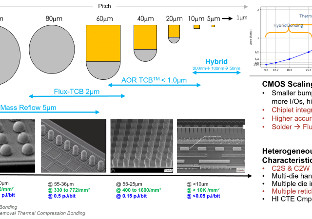
Enabling HBM 16H Stacks with Residue-Free Fluxless Active Oxide Removal
Using a plasma-based approach, active oxide removal technology empowers 3D chiplet integration and the HBM devices with fine bump pitch roadmaps and new package architectures.
U.S. Department of Commerce Announces CHIPS Incentives Awards with Corning, Edwards Vacuum, and Infinera
Today, the U.S. Department of Commerce announced it finalized three separate awards under the CHIPS Incentives Program’s Funding Opportunity for Commercial Fabrication Facilities.
Infinera’s Expansion Enhances Lehigh Valley’s Legacy of Technological Innovation
Infinera announced up to $93 million in federal funding to expand operations, including in the Lehigh Valley.