North America-based manufacturers of semiconductor equipment posted $2.32 billion in billings worldwide in June 2020 (three-month average basis), according to the June Equipment Market Data Subscription (EMDS) Billings Report published today by SEMI.
Packaging
Alchip Technologies 7nm ASIC Capabilities Set Advanced Technology Pace
With the number of expected tape outs jumping to nine by the end of 2020 Alchip Technologies, Limited has become one of the leading advanced technology ASIC providers. Alchip revealed that it had completed 3 tape outs in May alone.
GLOBALFOUNDRIES Partners with Synopsys, Mentor, and Keysight on Interoperable Process Design Kit (iPDK) Support for 22FDX
GLOBALFOUNDRIES (GF) today announced the release and distribution of OpenAccess iPDK libraries optimized for its 22FDX (22nm FD-SOI) platform. With its best-in-class performance, power consumption, and broad feature integration capability, GF’s differentiated 22FDX platform is the solution of choice for designers and innovators working in 5G mmWave, edge AI, Internet of Things (IoT), automotive, satellite communications, security, and other applications.
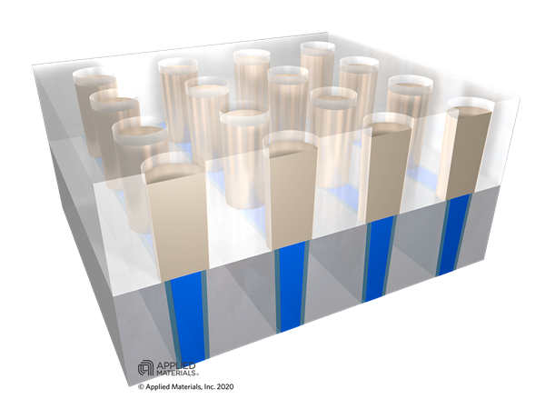
Applied Materials Solves Major Bottleneck to Continued 2D Scaling
Applied’s new Selective Tungsten process technology gives chipmakers a new way to build transistor contacts, which are the crucial, first level of wiring that connects the transistor to the rest of the wiring in the chip.
Applied Materials Charts a Course for Enabling a More Sustainable Company, Industry and World
In a keynote address today at the 50th annual SEMICON West, Applied Materials, Inc.president and CEO Gary Dickerson unveiled how the company is expanding the scope of its environmental, social and governance (ESG) commitments with a series of 10-year initiatives that will be driven within the company and in collaboration with suppliers, customers and the computing industry.
Aldec Provides Static Verification for RISC-V Designs with the Latest Release of ALINT-PRO
Aldec, Inc., a pioneer in mixed HDL language simulation and hardware-assisted verification for FPGA and ASIC designs, has added a RISC-V focused static verification rule set to ALINT-PROTM; rules that statically validate HDL code quality prior to simulation.
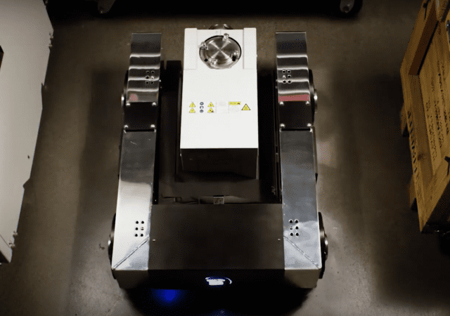
Edwards Vacuum Advanced Fab Robot Wins Best of West Award at Virtual SEMICON West 2020
The Edwards Service Vehicle X (ESV-X) concept automated mobile robot (AMR) – a reimagining of the semiconductor environment that features groundbreaking ground-up lifting and self-loading capabilities – today won the Best of West Award at the Virtual SEMICON West 2020.
SEMI Applauds Senate Support of Financial Incentives to Grow U.S. Semiconductor Manufacturing
SEMI President and CEO Ajit Manocha has voiced his support for amendments the United States House of Representatives and Senate included in the Fiscal Year 2021 National Defense Authorization Act (NDAA) that would authorize important programs to support semiconductor manufacturing and research in the U.S.
‘Standards Response’ to the Rescue: How Industry Specs Are Helping the Chip Industry Survive COVID
Announced today at SEMICON West 2020,when work around the world ground to a halt as humans sought to stop coronavirus, an unsurprising “essential” segment of the global economy proved capable of proceeding apace, keeping people employed and technology moving ahead.
Resilience of Chip Manufacturing Facilities During COVID-19 Rooted in SEMI Standards
Focusing in on how the microelectronics industry has proved capable of proceeding apace during the COVID-19 pandemic, SEMI today highlighted the role of industry standards and emerging developments around cybersecurity at the annual West Views Media Conference at SEMICON West 2020.