Synopsys, Inc. (Nasdaq: SNPS) today announced that Dr. John R. Rogers, principal engineer of imaging optics in the Optical Solutions Group at Synopsys, has been named the 2020 recipient of the SPIE Rudolf and Hilda Kingslake Award in Optical Design. SPIE, the international society for optics and photonics, presents the award in recognition of significant achievements in the field of optical design and optical engineering theory.
Packaging
SEMI 3D & Systems Summit Keynotes Spotlight 5G, HPC and System-in-Package Innovations
Top experts in 3D integration and systems for semiconductor manufacturing applications will gather at the SEMI 3D & Systems Summit, 27-29 January, 2020, in Dresden, Germany, for the latest developments and insights in 5G, High-Performance Computing (HPC), Heterogeneous Integration, 3D Roadmap and System-In-Package technologies. Global thought leaders from ASE Group, Huawei Technologies, TSMC and TechSearch International will headline the event with keynotes. Event registration is open.
Nepes Is Now Supplying a Highly Reliable Fan-Out Package to a Leading Wireless Chip Maker
Nepes (KOSDAQ: 033640), one of the top tier advanced packaging service providers, announces that it has initiated supply of high-reliability Fan-Out package service to a US based leading wireless chip maker. Fan-Out manufacturing is stabilized for mass production of the advanced package line recently acquired from Deca Technologies. “High Reliability Fan-out Package,” supplied by nepes, is a high-tech solution with more than 2 times BLR (Board Level Reliability) performance versus standard fan-out technologies by reducing physical stress on chips through sidewall protection structures.

Semiconductor Materials Growing to Nearly $50B Market in 2020 After Downturn
TECHCET—the electronic materials advisory services firm providing business and technology information— announced that global revenues for semiconductor manufacturing and packaging materials are expected to grow 5.7% year-over-year (YoY) in 2020 to US$49.5B, of which 65% represents semiconductor fab materials.
NY CREATES Begins Discussions on New Strategic Relationship With SEMI
The New York Center for Research, Economic Advancement, Technology, Engineering and Science (NY CREATES) today announced discussions to form a new Strategic Engagement with SEMI, the global industry association representing the electronics manufacturing and design supply chain. The announcement was made at the SEMI Industry Strategy Symposium, attended by several hundred C-Level semiconductor executives. Formed as a new and flexible industry interface in New York, NY CREATES is tasked with bridging academic, research, and industry innovation of the advanced electronics sector in New York.
EV/HEV Is Driving Power Electronics Innovations
The power electronics sector is pushing to adapt and propose innovative products. Objectives are clearly to answer to the specific needs coming from EV/HEV makers and make sure, for the power electronics companies, to be part of this attractive growth. They are so working on the miniaturization of the components, circuits and system design and are developing new solutions to integrate several systems in one system (e-axle, integration of DC-DC converter with a battery, etc.). Of course, WBG technologies are part of the technology roadmap, especially SiC power devices.
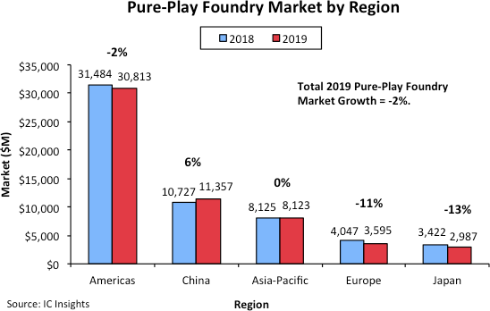
China Only Region to Register Pure-Play Foundry Market Growth in 2019
IC Insights is in the process of completing its forecast and analysis of the IC industry and will present its new findings in The McClean Report 2020, which will be published later this month. Among the semiconductor industry data included in the new 400+ page report is an in-depth analysis of the IC foundry market and its suppliers.
Growing Strained Crystals Could Improve Performance of Perovskite Electronics
A new method could enable researchers to fabricate more efficient and longer lasting perovskite solar cells, LEDs and photodetectors. By growing thin perovskite films on substrates with different compositions, engineers at the University of California San Diego have invented a way of fabricating perovskite single crystals with precisely deformed, or strained, structures. Engineering a small amount of strain in perovskites is of great interest because it provides a way to make significant changes in the material’s properties, such as how it conducts electricity, absorbs and transmits light, or how stable it is.
Inphi Surpasses Significant Milestone of 100,000 COLORZ Units Shipped
Inphi Corporation (NYSE: IPHI), a leader in high-speed data movement interconnects, today announced that it has shipped more than 100,000 COLORZ® units, the industry’s first lowest power and most cost effective 100G Silicon Photonics PAM4 platform solution for 80km DWDM connectivity in a QSFP28 form factor. The demand for bandwidth, driven by streaming video, social networking, cloud computing and mobile e-commerce, is motivating network operators to deploy cloud applications closer to the end users.
AI Chip Company Syntiant Joins Qualcomm Extension Program
Syntiant, an AI chip company providing custom always-on voice solutions at the edge, today announced that it is now a member of the Qualcomm® Extension Program, offering OEMs and ODMs accelerated integration of its ultra-low-power neural network technology with Qualcomm® Bluetooth audio platforms and SOCs. With support from the Qualcomm Extension Program, Syntiant plans to deliver a touch-free, cloud- free, machine learning voice solution for always-on speech applications in battery-powered devices, such as Bluetooth-enabled earbuds and hearable devices.