Polariton Technologies AG, an ETH Zurich spin-off, together with ETH Zurich have set a new benchmark in the field of electro-optic (EO) modulators with their latest innovation.
Packaging
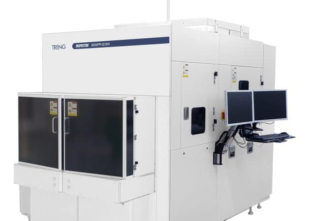
TASMIT Launches Large Glass Substrate Inspection System for Advanced Semiconductor Packaging
TASMIT Inc. has launched a new inspection system for glass substrates as part of its INSPECTRA series of semiconductor wafer visual inspection systems, which has gained attention for its high efficiency in advanced semiconductor manufacturing.
Saras Micro Devices Announces Participation in CHIPS National Advanced Packaging Manufacturing Program Initiatives
Saras Micro Devices today announced its participation in two significant projects funded by the U.S. Department of Commerce CHIPS National Advanced Packaging Manufacturing Program (NAPMP).
Semiconductor Climate Consortium Announces Key 2025 Initiatives
The Semiconductor Climate Consortium (SCC) today unveiled its four key initiatives for 2025, marking a significant step forward in advancing the industry’s commitment to decarbonization and transparency.
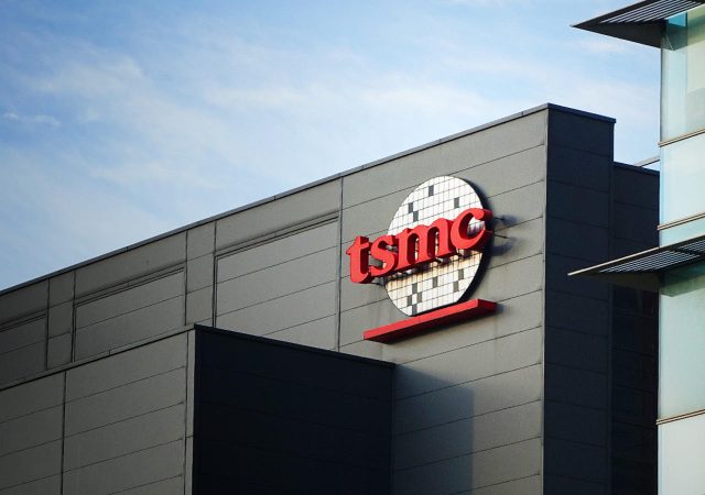
TSMC Intends to Expand Its Investment in the United States to US$165B
Company plans to increase U.S. investment in advanced semiconductor manufacturing by $100 billion with three new fabs, two advanced packaging facilities and an R&D center added to U.S. plans.
eInfochips Joins Samsung Advanced Foundry Ecosystem
eInfochips, an Arrow Electronics company, announced the company has joined the Samsung Advanced Foundry Ecosystem (SAFE) as a Virtual Design Partner.
sureCore PowerMiser IP Enables KU Leuven Chip for AI Applications to Achieve Dynamic Power Saving of Greater Than 40%
SureCore, the ultra-low power memory specialist, has enabled KU Leuven, Belgium’s renowned research university, to develop a neural processing accelerator chip for AI applications that boasts dynamic power savings in excess of 40%, compared to solutions using the industry standard SRAM.
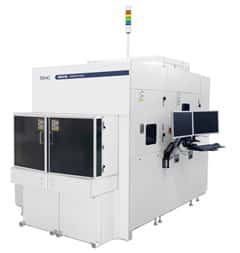
Launch of a Large Glass Substrate Inspection System for Advanced Semiconductor Packaging
TASMIT Inc. has developed a new inspection system for glass substrates as part of its INSPECTRA series of semiconductor wafer visual inspection systems, which has gained attention for its high efficiency in advanced semiconductor manufacturing.
Baya Systems and Semidynamics Collaborate to Accelerate RISC-V System-on-Chip Development
Baya Systems and Semidynamics today announced a collaboration to boost innovation in development of hyper-efficient, next-generation platforms for artificial intelligence (AI), machine learning (ML) and high-performance computing (HPC) applications.
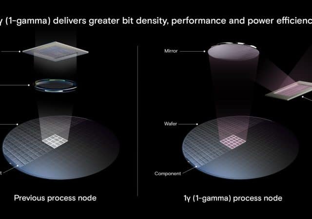
Micron Announces Shipment of 1γ (1-gamma) DRAM
Micron delivers superior performance and power efficiency to data center, client and mobile platforms with the industry’s first high performance 1γ node.