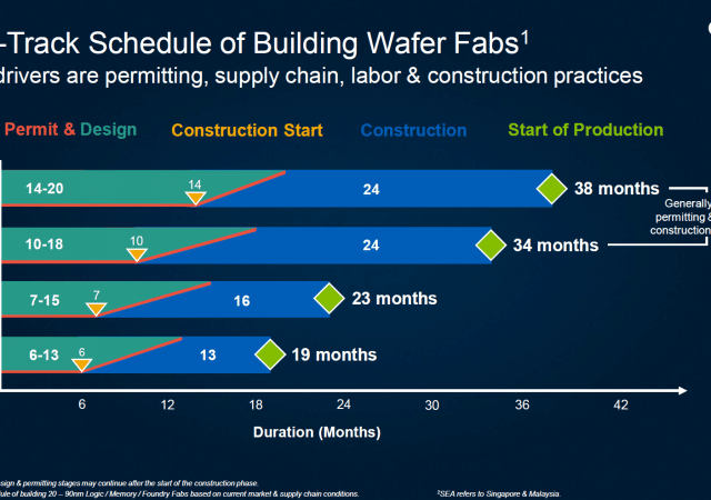
Construction costs in the U.S., compared to Taiwan, are about twice as much (the process equipment costs are similar). “Building a wafer fab in the west costs twice as much and takes twice the time of building it in Taiwan,” Exyte’s Blaschitz said at SEMI’s ISS.
Semiconductors
Gartner Says Worldwide Semiconductor Revenue Grew 18% in 2024
Worldwide semiconductor revenue in 2024 totaled $626 billion, an increase of 18.1% from 2023, according to preliminary results by Gartner, Inc. Revenue is projected to total $705 billion in 2025.
SEMI ISS Europe 2025 Speakers to Address AI, Sustainability, Supply Chain Resilience, and Workforce Development
The SEMI Industry Strategy Symposium Europe (ISS Europe) 2025, March 12-14 in Sopot, Poland, is themed AI: Catalyst to Propel Europe’s Competitiveness.
IKO’s New High-Thrust Linear Motor Stage Delivers Long Stroke Lengths in Constrained Spaces
IKO announced its LT170H2 direct drive linear motor stage for dynamic applications such as semiconductor fabrication which require high thrust forces and long strokes.
HUHUTECH Launches Kumamoto Warehousing and Logistics Center in Japan
HUHUTECH International Group Inc., a professional provider of factory facility management and monitoring systems, today announced the official opening of its semiconductor industry-supporting warehousing and logistics center located in Kumamoto Prefecture, Japan, through its Japanese subsidiary, HUHU Technology Co., Ltd.

What’s in the January/February Issue?
Each issue of Semiconductor Digest has articles found only in the magazine. Click on the links to read the articles in the January/February issue.

ULVAC Develops Roll-to-Roll Lithium Deposition System
ULVAC, Inc. announced the EWK-030, a roll-to-roll deposition system designed for lithium coating applications, scheduled for launch in May 2025.
Global Electronics and Semiconductor Materials Market to Reach $119.8 Billion by 2034
The electronics and semiconductor materials market is growing with AI, 5G, and automotive advancements. Key players like TSMC and Intel invest in SiC and GaN for high-performance chips.
ROHM’s New General-Purpose Chip Resistors Contribute to Greater Miniaturization
ROHM Semiconductor today announced an expanded portfolio of general-purpose chip resistors with the MCRx family, designed to achieve greater miniaturization and enhanced performance across a variety of applications.
Worldwide Silicon Wafer Shipments and Revenue Start Recovery in Late 2024, SEMI Reports
In the second half of 2024, worldwide silicon wafer demand started to recover from the industry downcycle seen in 2023, the SEMI Silicon Manufacturers Group (SMG) reported in its year-end analysis of the silicon wafer industry.
