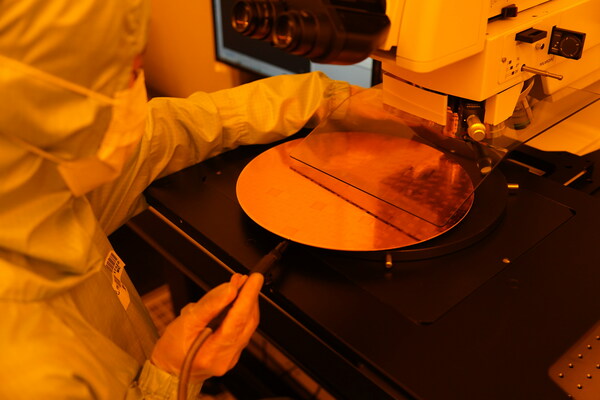
ClassOne Equipment announced the sale of its advanced new Takano WM-7SR particle measurement system to the DTU Nanolab at the Technical University of Denmark.
Semiconductors
Sourceability Launches Digital Pricing Solution for Managing Excess Inventory
Sourceability, a global distributor of electronic components, today announced the launch of its Excess Inventory Estimator.
Lam Research Introduces World’s First Bevel Deposition Solution to Increase Yield in Chip Production
Lam Research Corp. today introduced Coronus DX, the industry’s first bevel deposition solution optimized to address key manufacturing challenges in next-generation logic, 3D NAND and advanced packaging applications.
Applied Materials Charts Progress Towards Environmental, Social and Governance Goals in Latest Sustainability Report
Applied Materials, Inc. today announced the publication of its latest Sustainability Report, detailing its ESG (environmental, social and governance) initiatives and results over the past year.

ITRI Set to Strengthen Taiwan-UK Collaboration on Semiconductors
The newly established Department for Science, Innovation and Technology (DSIT) in the UK has recently released the UK’s National Semiconductor Strategy.
Intel, German Government Agree on Increased Scope for Wafer Fabrication Site in Magdeburg
Intel and the German federal government have signed a revised letter of intent for Intel’s planned leading-edge wafer fabrication site in Magdeburg, the capital of Saxony-Anhalt state in Germany.
RED Semiconductor Adds David Harold to Management Team
RED Semiconductor, a fabless semiconductor company, has added David Harold to the management team as Head of Business Development.
Vitesco Technologies and ROHM Sign a Long-Term SiC Supply Partnership
Vitesco Technologies, an international manufacturer of modern drive technologies and electrification solutions, has secured strategically important capacities in energy-efficient silicon carbide power semiconductors through a long-term supply partnership with ROHM – worth over one billion US dollars until 2030.
Extending Moore’s Law: CEA-Leti & Intel to Develop Atomically Thin 2D TMDs on 300mm Wafers Using Layer Transfer Technology for Future Transistor Scaling
CEA-Leti and Intel today announced a joint research project to develop layer transfer technology of two-dimensional transition-metal dichalcogenides (2D TMDs) on 300mm wafers with the goal to extend Moore’s Law beyond 2030.
Intel Plans Assembly and Test Facility in Poland
Investment near Wrocław, Poland, will help create a first-of-its-kind end-to-end leading-edge manufacturing semiconductor value chain in Europe.