D2S, a supplier of GPU-accelerated solutions for semiconductor manufacturing, today introduced the seventh generation of its computational design platform (CDP), a scalable processing solution for simulation-based semiconductor design and manufacturing applications.
Semiconductors
Process Technology Unveils the SHX Family of Products
Process Technology, a leading manufacturer of inline, ultra-high purity heaters for the semiconductor industry, is excited to announce its new family of SHX and SHX-EX heaters for IPA and flammable solvents.
South Korean Point Engineering Chooses ClassOne’s Solstice S8 for Advanced Semiconductor Plating
ClassOne Technology, global supplier of high-performance semiconductor electroplating and surface preparation systems, announced the sale of its Solstice S8 system to South Korean chip manufacturer, Point Engineering Co.
JEDEC Wide Bandgap Power Semiconductor Committee Publishes New Test Method for Continuous-Switching Evaluation of GaN Power Conversion Devices
JEDEC Solid State Technology Association, the global leader in standards development for the microelectronics industry, announces the publication of JEP182: Test Method for Continuous-Switching Evaluation of Gallium Nitride Power Conversion Devices.
Micron Delivers Industry’s First 1α DRAM Technology
Micron Technology today announced volume shipment of 1α (1-alpha) node DRAM products built using the world’s most advanced DRAM process technology and offering major improvements in bit density, power and performance.
ITRI and DuPont Jointly Inaugurate Semiconductor Materials Laboratory
Industrial Technology Research Institute (ITRI) and DuPont Electronics & Imaging (DuPont) today celebrated the opening of a new semiconductor materials laboratory in Hsinchu, Taiwan. DuPont established the laboratory to stay close to the semiconductor industry in Taiwan. DuPont will conduct, in collaboration with ITRI, semiconductor material research, development and enhancement, and accelerate pilot testing and commercial viability to support DuPont’s customers as they pursue the next generation of semiconductors in Taiwan. The evolution…
Amber Solutions Closes 2020 With Series B Funding Totaling More than $8.5 Million
Amber Solutions, the young Silicon Valley company that is making the digital control of electricity in solid-state architecture a commercial reality, today announced that its 2020 series B funding round raised more than $8.5 million from new and existing investors, following a successful year of secured patents, partner discussions and multiple industry award wins. According to Amber Founder and CEO Thar Casey, the company’s progress in 2020 is all the…
Titanium Oxide Nanotubes Facilitate Low-Cost Laser-Assisted Photoporation
A research team at the Department of Mechanical Engineering at Toyohashi University of Technology developed a nanosecond pulse laser-assisted photoporation method using titanium-oxide nanotubes (TNTs) for highly efficient and low-cost intracellular delivery.
indie Semiconductor Appoints David J. Aldrich to its Board of Directors
indie, an Autotech semiconductor and software innovator which is currently in the process of becoming a public company through a planned merger with Thunder Bridge Acquisition II.

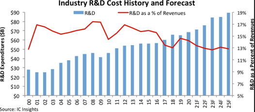
Industry R&D Spending to Rise 4% After Hitting Record in 2020
Intel stays on top of research and development ranking, but its share of total industry R&D expenditures dipped after its spending decreased 4% in 2020. AMD moved into the R&D top 10, says new report.