ACM Research, Inc. introduced alloy anneal capabilities for its Ultra Fn Furnace tool to extend its furnace product line to power device manufacturers.
Semiconductors
Onto Innovation Announces First Customer Qualification of New Aspect IRCD System
Onto Innovation Inc. today announced the first customer acceptance and purchase of its new product, the Aspect System, at one of the top three memory manufacturers of leading-edge 3D-NAND devices.
North American Semiconductor Equipment Industry Posts November 2020 Billings
North America-based manufacturers of semiconductor equipment posted $2.61 billion in billings worldwide in November 2020 (three-month average basis), according to the November Equipment Market Data Subscription (EMDS) Billings Report published today by SEMI.
No Security, No Safety
In a new webinar, Winbond’s Hung-Wei Chen provided an overview of today’s top cybersecurity threats and regulations, and detailed the company’s TrustME solutions for flash memory.
France Awards Soitec-led European Consortium for Semiconductor Innovation
The French Government has granted the REFERENCE consortium led by Soitec, a world leader in semiconductor materials based in France, the “Étoile de l’Europe” (“Star of Europe”) award for innovation in telecommunication.

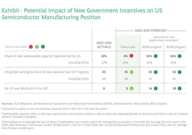
Semiconductor Manufacturing in the U.S.
In the middle of an ongoing pandemic and global trade war, the U.S. is looking to boost domestic semiconductor manufacturing capabilities.

Partially Hindered by the Pandemic, the MEMS Industry Could Emerge Stronger
Expect mixed effects in the 2020 MEMS market, followed by growth in the longer term.
SUEZ Unveils New Sievers TOC Analyzers for Online Ultrapure Water Monitoring
SUEZ – Water Technologies & Solutions announced the launch of two new Total Organic Carbon (TOC) online analyzers, the M500 for life sciences and the M500e for microelectronics markets.
CEA Combines 3D Integration Technologies & Many-Core Architectures to Enable High-Performance Processors That Will Power Exascale Computing
In an invited paper at IEDM 2020, CEA-List and CEA-Leti, research institutes at CEA, presented…
Combining Forces: LS Laser Systems and EPP Merge to Form L-TRIS
The Photonics Systems Group, a market leader in laser systems for micromaterial processing, is proud to announce the merger of two Group companies, LS Laser Systems and EPP Electronic Production Partners.