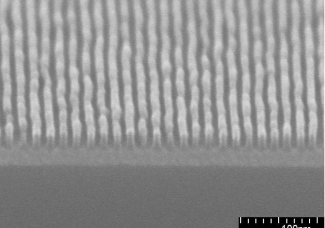
With shrinking dimensions, the classical lithography-based top-down patterning processes are becoming extremely complex and expensive. Therefore, researchers worldwide are investigating alternative processes allowing to build patterns from the bottom. Two promising approaches are directed self-assembly (DSA) and area-selective deposition (ASD).
Semiconductors

Deep Learning at the Extreme Edge: A Manifesto
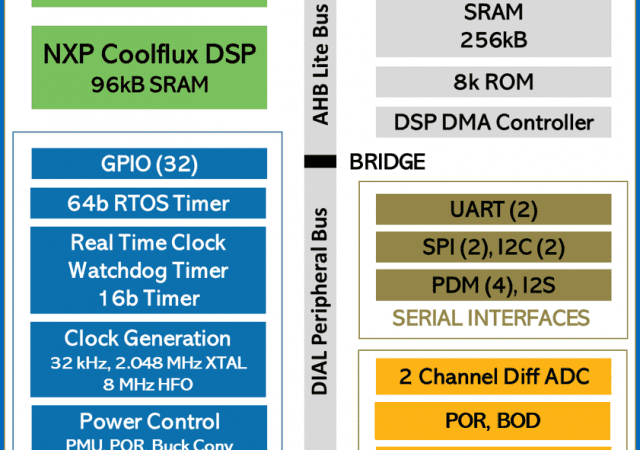
With continuous voltage and frequency scaling, the logic is self-timed, adjusting core voltage and clock frequency automatically, ensuring no timing violation. This allows the chip to always run the most efficient way for a given workload.
pSemi Welcomes New Vice President of Sales and Marketing, Vikas Choudhary
pSemi Corporation, a Murata company focused on semiconductor integration, today announces that Vikas Choudhary has joined the company as vice president of sales and marketing. Choudhary will lead pSemi’s worldwide sales, applications engineering, marketing, and marketing communications teams, and he will be responsible for driving pSemi’s unique RF, power, and sensor products into existing and emerging markets.
Cobham Advanced Electronic Solutions Appoints Mike Kahn as Chief Executive Officer
Cobham Advanced Electronic Solutions (CAES), a provider of mission critical electronic solutions, announces the appointment of Mike Kahn as Chief Executive Officer (CEO) effective September 1, 2020. Mike takes over from Shawn Black, who is leaving the business to pursue other opportunities.
MagnaChip Completes Sale of Foundry Services Group and Fab 4
MagnaChip Semiconductor Corporation announced that certain of its wholly owned subsidiaries have completed the previously announced sale of the Company’s Foundry Services Group and the factory in Cheongju to Key Foundry Co., Ltd.

Samsung Begins Mass Production of 16Gb LPDDR5 DRAM at World’s Largest Semiconductor Line
Samsung Electronics Co., Ltd., the world leader in advanced memory technology, today announced that its second production line in Pyeongtaek, Korea, has commenced mass production of the industry’s first 16-gigabit (Gb) LPDDR5 mobile DRAM, using extreme ultraviolet (EUV) technology.
Team’s Flexible Micro LEDs May Reshape Future of Wearable Technology
University of Texas at Dallas researchers and their international colleagues have developed a method to create micro LEDs that can be folded, twisted, cut and stuck to different surfaces.

CMP Consumables US$2.5B in 2020 for IC Fabs
TECHCET announces that the global market for chemical-mechanical planarization (CMP) consumable materials in semiconductor manufacturing is expected to total over US$2.5 billion this year.
Changes to Bosch Rexroth Management in North America
Paul Cooke, President and CEO of Bosch Rexroth North America, based in Charlotte, NC, USA, will retire on December 31, 2020 after 38 years of distinguished service in various international positions within Bosch Rexroth. His successor as of December 1, 2020 will be Greg Gumbs, most recently Vice President & General Manager Electrical Automation Solutions at EATON Corporation. Greg will join Bosch Rexroth effective September 1, 2020 in preparation for…
Photonics Researchers Report Breakthrough in Miniaturizing Light-Based Chips
Photonic integrated circuits that use light instead of electricity for computing and signal processing promise greater speed, increased bandwidth, and greater energy efficiency than traditional circuits using electricity.
