Just as a meter stick with hundreds of tick marks can be used to measure distances with great precision, a device known as a laser frequency comb, with its hundreds of evenly spaced, sharply defined frequencies, can be used to measure the colors of light waves with great precision.
Semiconductors
EU Team Demonstrates Full Data-Transfer Silicon Photonics Module Delivering 100 Gb/s and Develops Building Blocks for Tb/s
CEA-Leti today announced the demonstration of a fully packaged CWDM optical transceiver module with data transfer of 100 Gb/s per fiber with a low-power-consumption electronic chip co-integrated on the photonic chip. This silicon-photonics-based transceiver multiplexes two wavelengths at 50 Gb/s and is designed to meet the ever-increasing data-communication demands and energy use of data centers and supercomputers.

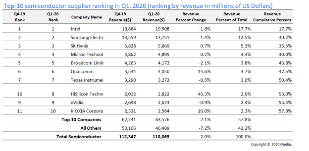
Top-10 Semiconductor Suppliers Defy Weak Market Conditions in Q1
Defying a decline in market revenue, the world’s top-10 semiconductor suppliers managed to generate revenue growth of 2.1 percent in the first quarter, as the companies benefitted from a COVID-19-driven increase in PC and server sales.
GLOBALFOUNDRIES to Acquire Land in Malta, NY
GLOBALFOUNDRIES today announced it has secured a purchase option agreement for approximately 66 acres of undeveloped land adjacent to its most advanced manufacturing facility, Fab 8, in Malta, N.Y., near the Luther Forest Technology Campus (LFTC).
NY CREATES Announces New AIM Leadership
NY CREATES (New York Center for Research, Economic Advancement, Technology, Engineering and Science) announce the appointment of Dr. Michael J. Cumbo as Chief Executive Officer (CEO) for the American Institute for Manufacturing Integrated Photonics (AIM Photonics), a program of NY CREATES, effective July 6, 2020.
Semtech Announces Production of New Tri-Edge, a PAM4 CDR Platform for 200G and 400G Data Center Applications
Semtech Corporation (Nasdaq: SMTC), a leading supplier of high performance analog and mixed-signal semiconductors and advanced algorithms, today announced production availability of GN2558 and GN2559, Semtech’s Tri-Edge CDR SR solutions to enable next-generation data center multi-mode interconnectivity.
SEMI Virtual Summit Focuses on Microtechnology-Enabled Solutions to Healthcare Challenges
The latest healthtech innovations driven by microelectronics will be presented at the SEMI Virtual Healthtech Summit, Europe’s first online event to explore the critical role of semiconductors in solving the world’s most pressing healthcare challenges including COVID-19. Registration is open for the July 16, 2020, summit.
Measuring a Tiny Quasiparticle Is a Major Step Forward for Semiconductor Technology
A team of researchers led by Sufei Shi, an assistant professor of chemical and biological engineering at Rensselaer Polytechnic Institute, has uncovered new information about the mass of individual components that make up a promising quasiparticle, known as an exciton, that could play a critical role in future applications for quantum computing, improved memory storage, and more efficient energy conversion.
North American Semiconductor Equipment Industry Posts May 2020 Billings
North America-based manufacturers of semiconductor equipment posted $2.35 billion in billings worldwide in May 2020 (three-month average basis), according to the May Equipment Market Data Subscription (EMDS) Billings Report published by SEMI.
Call for SEMICON West 2020 “Best of West” Award Applications
SEMI today began accepting SEMICON West 2020 exhibitor applications for the Best of West award recognizing innovative new products or services that are significantly advancing the electronics manufacturing supply chain or a particular manufacturing capability.