Intel Corporation today announced that Dion J. Weisler, former president and CEO of HP Inc., was elected to Intel’s board of directors. Weisler will serve as an independent director and member of the compensation and finance committees.
Semiconductors

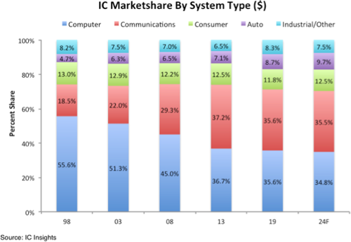
Automotive IC Market Forecast With Strongest CAGR Through 2024
IC Insights released its June Update to the 2020 McClean Report earlier this month. This Update included a 2018-2024 IC database that segmented the IC market by major product type including Consumer, Auto, Computer, Industrial, Communications, and Government/Military end-use applications in the Americas, Europe, Japan, China, and Asia-Pacific regions.
Excitons Form Superfluid in Certain 2D Combos
Mixing and matching computational models of 2D materials led scientists at Rice University to the realization that excitons — quasiparticles that exist when electrons and holes briefly bind — can be manipulated in new and useful ways.
Cadence Collaborates With TSMC and Microsoft to Reduce Semiconductor Design Timing Signoff Schedules With the Cloud
Cadence Design Systems, Inc. (Nasdaq: CDNS) today announced the results of a three-way collaboration with TSMC and Microsoft focused on utilizing cloud infrastructure to reduce semiconductor design signoff schedules.
Discovery of Graphene Switch
Researchers at Japan Advanced Institute of Science and Technology (JAIST) have successfully measured the current-voltage…
QuickLogic Announces Open Reconfigurable Computing Initiative
QuickLogic Corporation today announced its ground breaking QORC (QuickLogic Open Reconfigurable Computing) initiative, making it the first programmable logic vendor to actively embrace a fully open source suite of development tools for its FPGA devices and eFPGA technology.
GaN Systems Announces Sixth Annual “GaN Systems Cup” China Power Supply Society Design Competition
GaN Systems, the global leader in GaN (gallium nitride) power semiconductors, is proudly sponsoring the distinguished China Power Supply Society (CPSS) design competition, which focuses on innovation in energy conservation, emission reduction, and new energy utilization.
Bipartisan, Bicameral Bill Will Help Bring Production of Semiconductors, Critical to National Security, Back to U.S.
U.S. Sen. Mark R. Warner (D-VA), Vice Chairman of the Senate Select Committee on Intelligence, and Sen. John Cornyn (R-TX) introduced the Creating Helpful Incentives to Produce Semiconductors (CHIPS) for America Act.
NXP Selects TSMC 5nm Process for Next Generation High Performance Automotive Platform
NXP Semiconductors N.V. (NASDAQ: NXPI) and TSMC (TWSE: 2330, NYSE: TSM) today announced a collaboration agreement to adopt TSMC’s 5-nanometer (5nm) technology for NXP’s next generation, high-performance automotive platform.
SEMI Announces Support of CHIPS for America Act to Increase Semiconductor Manufacturing in the U.S.
The bipartisan legislation would improve the competitiveness of semiconductor research, design and manufacturing in the United States, resulting in the creation of thousands of new jobs and bolstering national security.