Ereztech, a leading provider of complete metal-organic solutions to the semiconductor industry, today announced the opening of its new research and development (R&D) lab in Sheboygan Falls, Wisconsin.
Semiconductors
Keysight Technologies’ Combines Technology and Solutions Expertise to Deliver the New Infiniium MXR-Series Mixed Signal Oscilloscopes
Keysight Technologies, Inc. (NYSE: KEYS), a leading technology company that helps enterprises, service providers and governments accelerate innovation to connect and secure the world, announced the first oscilloscope with 8 analog channels at 6 GHz and 16 simultaneous digital channels, enabling customers to reduce test bench and workflow complexity to achieve higher performance as well as accurate and repeatable multi-channel measurements in a single instrument.
Samsung Unveils Innovative Storage Technology at OCP Virtual Global Summit
Samsung announced today in an OCP Virtual Summit keynote that it has developed a solid state drive (PM9A3 SSD) with a SNIA-based* E1.S form factor and full PCIe Gen 4 support to harness the production efficiencies of the company’s sixth-generation (1xx-layer), three-bit V-NAND. At the same time, the company said that it has introduced a comprehensive reference design for its E1.S-based storage system.
COVID-19: The Way Forward – Insights from McKinsey & Company
In much of post-lockdown China, urban life is humming. Streets in Beijing and Shanghai are bustling with traffic, smog again shrouds city skylines with the resurgence of economic activity, property sales are bouncing back and a revival in consumer confidence is taking hold. Emerging from monthslong shelter-in-place orders, the nation has seized a large measure of control in containing COVID-19 as it breaks fertile new ground in pandemic response and recovery.
Eta Compute Partners with Edge Impulse to Accelerate the Development and Deployment of Machine Learning at the Edge
Eta Compute and Edge Impulse announce that they are partnering to accelerate the development and deployment of machine learning using Eta Compute’s revolutionary ECM3532, the world’s lowest power Neural Sensor Processor, and Edge Impulse, the leading online TinyML platform. The partnership will speed the time-to-market for machine learning in billions of IoT consumer and industrial products where battery capacity has been a roadblock.
Heilind Electronics and Laird Performance Materials Sign Global Distribution Agreement
Heilind Electronics, a leading distributor of electronic components, announced today the signing of a global distribution agreement with Laird Performance Materials, a portfolio company of privately held Advent International.
Pfeiffer Vacuum Supplies Turbopumps for GANIL Large-Scale Research Facility in France
Pfeiffer Vacuum has received several major orders from the French large-scale research facility GANIL (Grand Accélérateur National d’Ions Lourds) (National Large Heavy Ion Accelerator) for the supply of turbopumps and custom vacuum chambers.
Pure Wafer Expands Production Capacity at AZ and CA Facilities Announces New Films Services Group to Meet Semi R&D Needs
Pure Wafer, America’s leading provider of reclaimed wafers and thin films services to the semiconductor manufacturing industry announced today that it has expanded production at its Arizona and California facilities.

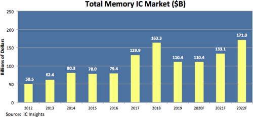
Memory Market Not Forecast to Exceed 2018 High of $163.3B until 2022
The most current 2017-2024 forecast for 35 major IC product segments (e.g., DRAM, 16-bit MCUs, power management analog devices, etc.) by market, unit shipments, and ASP was presented in the April Update to the 2020 edition of The McClean Report—A Complete Analysis and Forecast of the Integrated Circuit Industry (MR20).
2D Oxide Flakes Pick Up Surprise Electrical Properties
Rice University researchers have found evidence of piezoelectricity in lab-grown, two-dimensional flakes of molybdenum dioxide. Their investigation showed the surprise electrical properties are due to electrons trapped in defects throughout the material, which is less than 10 nanometers thick.