By taking its core capabilities in manufacturing and design of nanocarbon materials for optics and semiconductor electronics systems, AKHAN will leverage its expertise and fabrication capabilities to alleviate the existing bottleneck in Bio-FET device systems.
Semiconductors
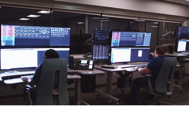
Data-Center Switching Market to Plunge Nearly 10% in the First Half as Coronavirus Ravages the Supply Chain
While the market for data-center switches is experiencing both positive and negative impacts from the coronavirus crisis, the net effect of the pandemic will be a 3 to 4 percent reduction in revenue and ports during the first half of 2020 compared to previous expectations.
Windows Will Soon Generate Electricity, Following Solar Cell Breakthrough
Semi-transparent solar cells that can be incorporated into window glass are a “game-changer” that could transform architecture, urban planning and electricity generation, Australian scientists say in a paper in Nano Energy. The researchers – led by Professor Jacek Jasieniak from the ARC Centre of Excellence in Exciton Science (Exciton Science) and Monash University – have succeeded in producing next-gen perovskite solar cells that generate electricity while allowing light to pass through.…
IDC Forecasts a Drop in IT Spending in Nearly Every Industry in 2020 Due to COVID-19
International Data Corporation (IDC) currently forecasts worldwide IT spending to decline 2.7% this year due to the economic impact of the COVID-19 pandemic. While every industry will be affected by the global slowdown, some will reduce their IT spending more than others. In the first of several special releases to the Worldwide ICT Spending Guide: Industry and Company Size, IDC provides an industry-level assessment of how COVID-19 will impact IT spending.
Tektronix Adds Industry-First Technology Which Eliminates Pulse Tuning in New All-In-One 2601B-PULSE System SourceMeter
Tektronix, Inc. today announced the new 2601B-PULSE System SourceMeter® 10μs Pulser/SMU Instrument, integrating a high-speed current pulser with DC source and measurement functions in one instrument.
SiPearl Signs a Major Licensing Agreement with Arm
SiPearl, the company that is designing the high-performance, low-power microprocessor for the European exascale supercomputer, has signed a major technological licensing agreement with Arm, the global semiconductor IP provider. The agreement will enable SiPearl to benefit from the high-performance, secure, and scalable next-generation Arm® Neoverse™ platform, codenamed ‶Zeusʺ, as well as leverage the robust software and hardware Arm ecosystem.
Sponsorship of Women Helps Address Talent Gap and Increase Profitability in Semiconductor Companies, SEMI Report Finds
A new report from SEMI, the industry association serving the global electronics manufacturing and design supply chain, highlights how sponsorship programs can help the semiconductor industry tackle its talent gap and increase profitability.
High-Quality Boron Nitride Grown at Atmospheric Pressure
Graphene Flagship researchers at RWTH Aachen University, Germany and ONERA-CNRS, France, in collaboration with researchers at the Peter Grunberg Institute, Germany, the University of Versailles, France, and Kansas State University, US, have reported a significant step forward in growing monoisotopic hexagonal boron nitride at atmospheric pressure for the production of large and very high-quality crystals.
Terahertz Science Discloses the Ultrafast Photocarrier Dynamics in Carbon Nanotubes
A team of researchers from Osaka University, TU Wien, Nanyang Technological University, Rice University, University of Alberta and Southern Illinois University-Carbondale comes closer to unraveling the physics of quasiparticles in carbon nanotubes.
Intel Commits $50M with Pandemic Response Initiative to Combat Coronavirus
Today, Intel is pledging an additional $50 million in a pandemic response technology initiative to combat the coronavirus through accelerating access to technology at the point of patient care, speeding scientific research and ensuring access to online learning for students.