In response to the COVID-19 pandemic, Intel announced Monday that it will source and donate more than 1 million items of personal protective equipment – masks, gloves and other gear – to healthcare workers.
Semiconductors
Clemson Researcher’s Novel MOF Is Potential Next-Gen Semiconductor
Metal-organic frameworks (MOFs) are emerging multi-functional materials that are gradually finding their way out of the research labs and into a myriad of real-world applications. For example, MOFs can store dangerous gasses, catalyze chemical reactions, deliver drugs in controlled fashion, and may even be used in rechargeable batteries and solar cells.
BrainChip and Socionext Provide a New Low-Power Artificial Intelligence Platform for AI Edge Applications
BrainChip Holdings Ltd (ASX: BRN), a leading provider of ultra-low power high performance AI technology today announced that Socionext Inc., a leader in advanced SoC solutions for video and imaging systems, will offer customers an Artificial Intelligence Platform that includes the Akida SoC, an ultra-low power high performance AI technology.
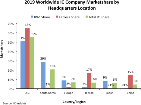
U.S. IC Companies Maintain Global Marketshare Lead
Propelled by 51% share of IDM sales and 65% share of fabless sales, U.S. companies captured 55% of the total worldwide IC market in 2019.
North American Semiconductor Equipment Industry Posts February 2020 Billings
North America-based manufacturers of semiconductor equipment posted $2.37 billion in billings worldwide in February 2020 (three-month average basis), according to the February Equipment Market Data Subscription (EMDS) Billings Report published today by SEMI. The billings figure is 1.2 percent higher than the final January 2020 level of $2.34 billion, and is 26.2 percent higher than the February 2019 billings level of $1.88 billion.
COVID-19 To Have Significant Effect on Worldwide Semiconductor Market in 2020, According to IDC
The Coronavirus Disease 2019 (COVID-19) is affecting China and is spreading within East Asia and into Europe and North America. In addition to the human cost of life, the impact of the spread of the virus on the global economy is only beginning to be appreciated and has deep implications for the world’s technology supply chain. A new International Data Corporation (IDC) report, Impact of COVID-19 on the Worldwide Semiconductor Market Forecast (IDC #US46115520), provides IDC’s view on the impact the COVID-19 virus will have on the semiconductor market.
A Nanoscale Laser Made of Gold and Zinc Oxide
Tiny particles composed of metals and semiconductors could serve as light sources in components of future optical computers, as they are able to precisely localize and extremely amplify incident laser light. A team from Germany and Sweden led by Prof. Dr. Christoph Lienau and Dr. Jin-Hui Zhong from the University of Oldenburg has now explained for the first time how this process works. The study is published in the current issue of the journal Nature Communications.
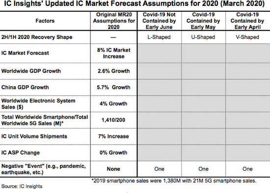
“Black Swan” Event Triggers Revision to 2020 IC Market Forecast
The recent surge of the spread of the coronavirus (Covid-19) and its anticipated negative impact on the global economy and IC market definitely fits the definition of a Black Swan event.
Semiconductors Can Behave Like Metals and Even Like Superconductors
The crystal structure at the surface of semiconductor materials can make them behave like metals and even like superconductors, a joint Swansea/Rostock research team has shown. The discovery potentially opens the door to advances like more energy-efficient electronic devices. Semiconductors are the active parts of transistors, integrated circuits, sensors, and LEDs. These materials, mostly based on silicon, are at the heart of today’s electronics industry.
Novel Approach to Enhance Performance of Graphitic Carbon Nitride
In a report published in NANO, scientists from the Jiangxi University of Science and Technology, Guangdong University of Petrochemical technology, Gannan Medical University and Nanchang Hangkong University in China underline the importance of defect engineering to promote catalytic performance by providing a simple and efficient way for modifying and optimizing metal-free semiconductor photocatalyst graphitic carbon nitride (g-C3N4) to solve the dual problems of environmental pollution and lack of fossil resources.