ClassOne Technology, global supplier of advanced electroplating systems for ≤200mm wafer processing, announced the sale of its Solstice® S4 system to the Ferdinand-Braun-Institut (FBH) in Berlin. The FBH is a major III-V compound semiconductor research institute that develops leading-edge microwave and optoelectronic devices for communications, energy, health, mobility and other industries.
Semiconductors
New SEMI Job Skills Model for Growing Microelectronics Industry Talent Pipeline Released by U.S. Department of Labor – Employment and Training Administration
SEMI today announced the release of a central feature of its workforce development initiative, designed to grow the microelectronics industry’s talent pipeline, on the U.S. Department of Labor’s Competency Model Clearinghouse website. The Unified Competency Model (UCM) for Advanced Manufacturing identifies skill sets required across strategic industry sectors to strengthen connections among the microelectronics industry, workers, and education and training providers.
Room-temperature Bonded Interface Improves Cooling of Gallium Nitride Devices
A room-temperature bonding technique for integrating wide bandgap materials such as gallium nitride (GaN) with thermally conducting materials such as diamond could boost the cooling effect on GaN devices and facilitate better performance through higher power levels, longer device lifetime, improved reliability, and reduced manufacturing costs.

Finding Wafers Just Got Much Easier
Inseto launches comprehensive online store for selecting and ordering silicon, silica, glass, coated and SOI wafers.

The Need for IoT Security At the Chip Level
A critical element to successful IoT security chips is public key infrastructure (PKI). All IoT devices with these chips require a strong identity, which will then be used for secure authentication.
MISUMI to Relocate North American HQ to Schaumburg Corporate Center
MISUMI, a global supplier of configurable components, is excited to announce the relocation of its North American corporate headquarters to Glenstar’s Schaumburg Corporate Center located at 1475 E. Woodfield Road. Located adjacent to Woodfield Mall, the total property is a 1 million-square-foot, three-building office complex. MISUMI plans to take occupancy in June 2020.
Water-Free Way to Make MXenes Could Mean New Uses for the Promising Nanomaterials
Ten years after producing the first sample of the now widely studied family of nanomaterials, called MXenes, Drexel University researchers have discovered a different way to make the atom-thin material that presents a number of new opportunities for using it. The new discovery removes water from the MXene-making process, which means the materials can be used in applications in which water is a contaminant or hampers performance, such as battery electrodes and next-generation solar cells.
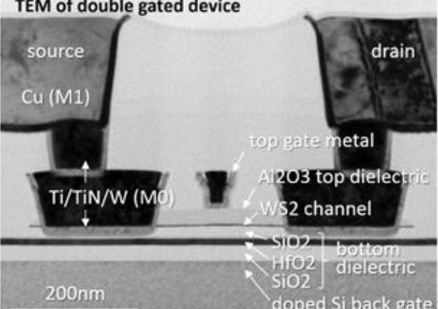
A 300mm Platform for 2D-Material Based MOSFET Devices
2D materials, a family of materials that form two-dimensional crystals, promise to enable a broad range of semiconductor applications, such as selectors or back-end compatible transistors.
Advent of 5G and AI Chip Manufacturing Renews the Need for Advanced Semiconductor Testing Systems
A surge in semiconductor test volumes and stringent test demands from the communication, consumer electronics, automotive and healthcare verticals are expected to revive the semiconductor industry following a sharp decline in revenues for the global semiconductor automated test equipment market in 2019.
EUV Materials Small But Strategic Fraction of $1.6B IC Photoresists Market
The global market for Photoresists and Ancillary Materials declined in 2019 due to semiconductor fabrication market challenges.